Reverse Engineering
Reverse engineering of Printed circuit boards (sometimes called “cloning”, or PCB RE) is the process of generating fabrication and design data for an existing circuit board, either closely or exactly replicating its functionality
Reverse-Engineering Methods
Destructive RE
Destructive reverse engineering (DRE) is a process where all layers of the board are imaged and subsequently removed by various milling techniques or tools.
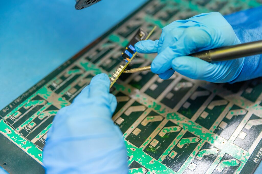
Non-Destructive RE
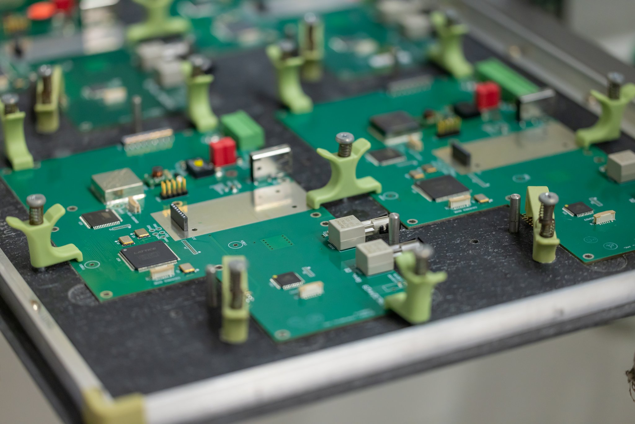
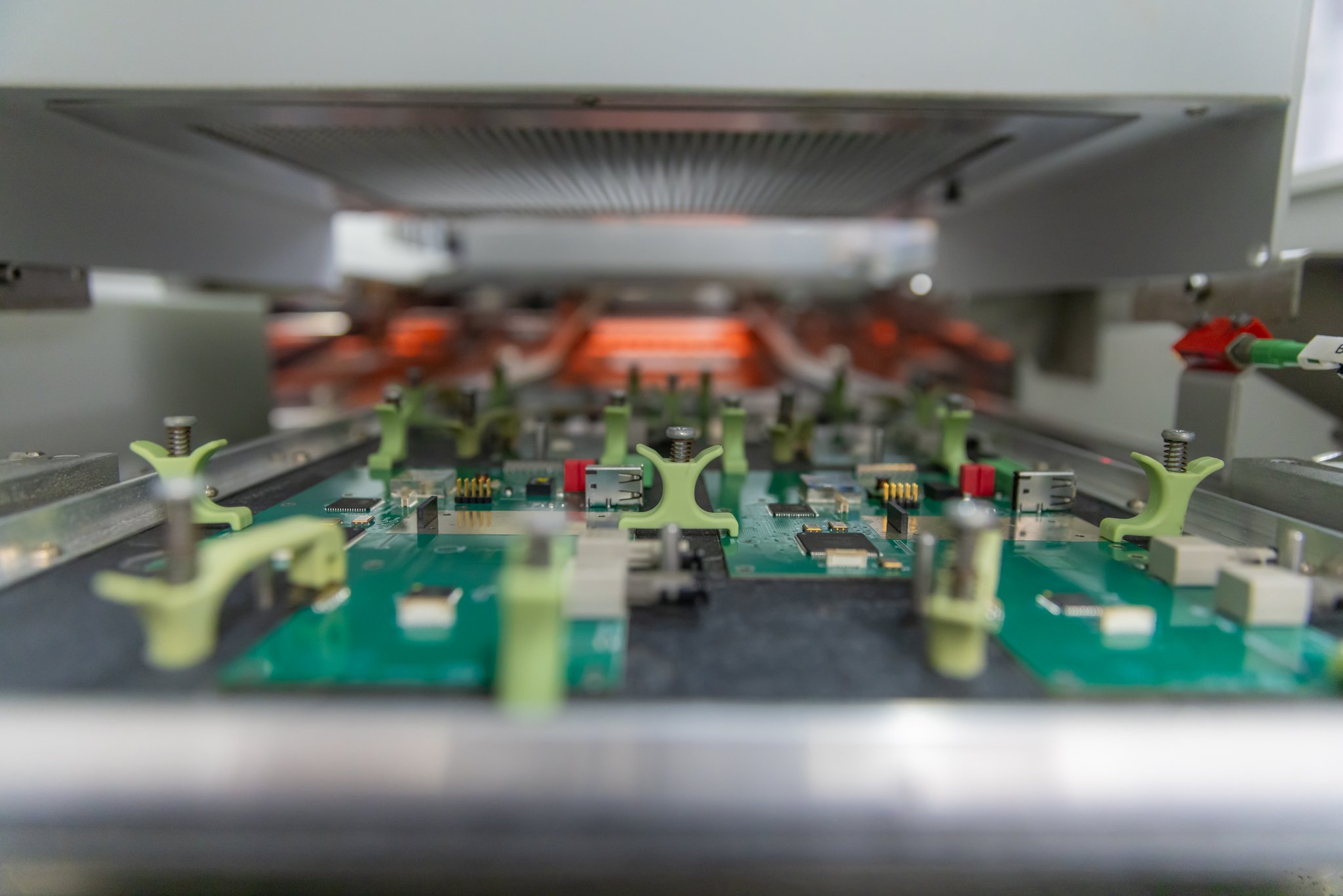
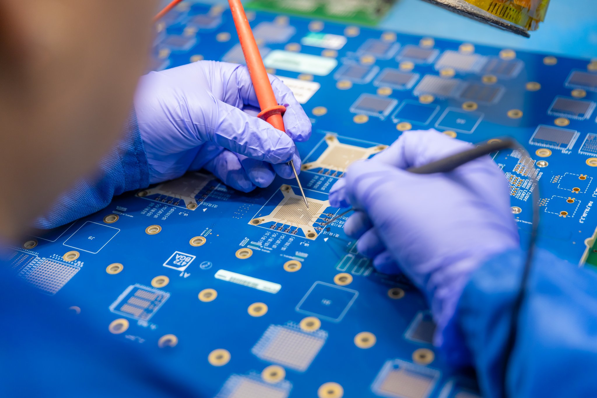
Non-destructive PCB RE (NDRE) mean that the circuit board itself is not destroyed in the process. however, most non-destructive techniques require removing components from the surface of the board.
X-ray Computed Tomography
X-ray computed tomography-based imaging processes have advanced to the point that they are able to capture images of the circuit board well enough to isolate individual layers and the features on each of these layers
Flying Probe Test
Oftentimes a Flying Probe test machine (FPT machine) can also be used to generate data from a circuit board. Unlike destructive methods, with this process the PCB can generally be reused.
X-ray imaging
In addition, a schematic can be merged with the Bill of Materials (BOM) and component Pick and Place data to further enhance its usability in troubleshooting scenarios, or can be used as a base for the design of a brand new PCB. If a destructive RE process has been used or images for all PCB layers have been captured using X-ray imaging
Final outputs and reproduction
Whether the board is reverse engineered using a destructive or non-destructive method, the result is that a netlist is obtained. While the netlist itself cannot be used to create an identical replacement, it can be used to generate supporting data for the board like a schematic.
Legacy product support
Legacy systems need maintenance and replacement parts to operate past their intended life cycle. Demand for parts that are no longer being manufactured can lead to material shortages of parts, called DMS/DMSMS.
Industries We Serve:
How It Works
Circuit layers
The PCB stack-up design clearly defines each and every layer and its order, there should be physical labels on each layer for their accurate placement.
Soldermask and Solderpaste
solder mask is the material applied to the circuit board to protect it and paste mask is the pattern used to apply the solder paste
Drill files
NC Drill File is also known as numeric control drill file. This indicates a file that regulates all the information relating to via or hole drilling requirements.
Plated and NonPlated Through-holes
The plating on the through holes is copper, a conductor, so it allows electrical conductivity to travel through the board. Non-plated through holes do not have conductivity,
Per-layer Blind
Blind vias are essential for multilayer PCBs, allowing efficient and reliable connections between the various layers without resorting to traditional through-hole vias that span the entire board.
BOM
A PCB bill of materials (BOM) is a comprehensive list that provides information on all the components to be assembled on your board.
PCB Reverse engineering Advantages
- Remanufacturing of Obsolete PCBs
- PCB Repairs
- Modifications or Improvements
- Interoperability Design
One of the primary benefits of PCB reverse engineering is its ability to recreate discontinued or obsolete PCBs. In many cases, the original equipment manufacturer (OEM) may no longer provide support or replacement parts for older equipment.
PCBs can develop faults and failures over time due to various reasons, including wear and tear, component degradation, or environmental factors. Understanding the design and components of a PCB through reverse engineering simplifies the diagnosis of faults.
Reverse engineering provides engineers with detailed schematics and a comprehensive understanding of a PCB’s design. This knowledge empowers them to suggest and implement custom modifications or improvements to the PCB
Reverse engineering can provide valuable insights into the inner workings of competitors’ products. Analyzing these products allows engineers to gain a deeper understanding of their design choices and functionality
Our Certifications