Our HDI PCB Fabrication Services are designed to manufacture high-performance printed circuit boards with exceptional precision, reliability, and density. Using advanced fabrication technologies such as laser-drilled microvias, blind and buried vias, sequential lamination, and fine-line circuitry, we produce HDI PCBs that meet the demanding requirements of modern electronic devices. From prototypes to high-volume production, our IPC-compliant manufacturing processes ensure superior electrical performance, enhanced signal integrity, and consistent product quality across every build.
Our HDI PCB fabrication services enable manufacturers to develop smaller, lighter, and more powerful electronic products without compromising reliability.
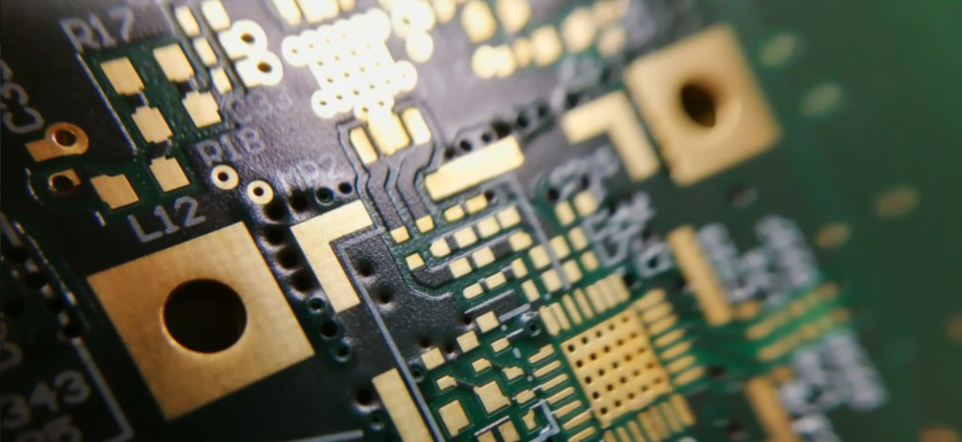
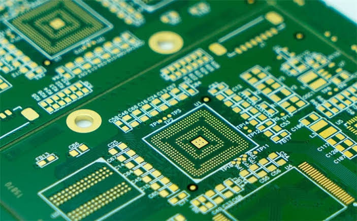
We fabricate 1+N+1, 2+N+2, and any-layer HDI PCBs for applications requiring compact designs and complex interconnections. Our capabilities include microvia drilling, via-in-pad technology, controlled impedance, high-density routing, stacked and staggered vias, fine-pitch fabrication, and high-speed PCB manufacturing. Every board is engineered to maximize routing efficiency while minimizing size, weight, and signal loss for next-generation electronic products.
Every HDI PCB undergoes rigorous quality inspections throughout the fabrication process. We utilize Automated Optical Inspection (AOI), X-ray inspection, electrical testing, impedance verification, and flying probe testing to ensure every circuit board meets IPC standards and customer specifications. Our experienced engineering team also performs Design for Manufacturing (DFM) reviews to optimize production efficiency, reduce manufacturing risks, and improve first-pass yield.
With decades of experience in advanced PCB fabrication, Altest Corporation delivers reliable HDI manufacturing solutions for medical devices, aerospace, defense, telecommunications, automotive, industrial automation, and consumer electronics. Our state-of-the-art manufacturing processes, strict quality control, and engineering expertise enable us to produce complex HDI PCBs with faster turnaround times, competitive pricing, and exceptional reliability. Whether you need a rapid prototype or large-scale production, we provide complete end-to-end support to help bring your high-density electronic products to market with confidence.
Find answers to common questions about High-Density Interconnect technology, microvias, sequential lamination, and routing solutions for ultra-fine pitch components.
HDI PCBs are circuit boards designed with a significantly higher wiring density per unit area than conventional boards. They achieve this by utilizing laser-drilled microvias, blind and buried vias, and ultra-fine trace widths. This allows engineers to pack more functionality into much smaller, lighter form factors, essential for modern wearables, aerospace modules, and mobile devices.
Standard vias are mechanically drilled, typically 8 mils (0.2mm) or larger, and usually pass completely through all layers of the board. Microvias are precision laser-drilled, generally 6 mils (0.15mm) or smaller in diameter, and only span across one or two adjacent layers at a time. This targeted routing frees up massive amounts of real estate on the remaining layers.
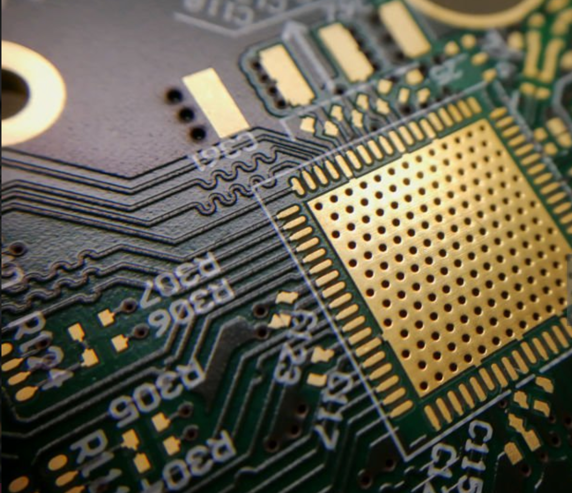
Via-in-Pad places the via directly underneath the component's surface contact pad, rather than routing a trace outward to a standard via. We plate these vias shut, fill them with conductive or non-conductive epoxy, and planarize (flatten) the surface. This technique saves critical surface space and minimizes trace inductance, making it mandatory for routing high-pin-count, fine-pitch BGAs.
Beyond drastically reducing the size and weight of the physical board, HDI improves electrical performance. The shortened signal paths achieved through microvias reduce signal reflections, cross-talk, and parasitic capacitance/inductance. This leads to cleaner, faster signal transmission, which is critical for high-speed digital architectures.
Yes. For highly complex designs (like Any-Layer HDI), we utilize both staggered and stacked microvias. Stacked microvias are placed directly on top of each other across multiple sequential layers, while staggered vias are offset. We use highly controlled laser drilling and solid copper plating techniques to ensure structural reliability and prevent via cracking in these advanced structures.
HDI boards require "sequential lamination"—meaning the board is pressed, drilled, and plated multiple times to build up the complex inner structures. Because of these additional manufacturing cycles and specialized laser drilling, HDI boards have a higher initial fabrication cost and longer lead time than standard boards. However, they often reduce total system cost by consolidating multiple boards into a single unit.
While standard High-Tg FR-4 can be used for basic HDI, we strongly recommend advanced, dimensionally stable materials with a low Coefficient of Thermal Expansion (CTE). Specialized substrates from Isola, Panasonic, or Rogers help prevent microvia barrel cracking and pad lifting during the multiple heat cycles required for sequential lamination and SMT reflow.
For advanced HDI fabrication, our Silicon Valley facility utilizes Laser Direct Imaging (LDI) to achieve ultra-fine trace widths and spacing down to 2.0 mils / 2.0 mils (and tighter for specialized IC substrates). This precision is absolutely critical when "fanning out" traces from high-pin-count BGA components with pitches of 0.4mm or below.
We ensure via reliability through rigorous, non-destructive and destructive testing protocols. This includes High-Resolution 3D X-Ray (AXI) inspection, destructive microsection (cross-section) analysis of test coupons, and thermal shock testing. This guarantees that the copper plating inside the stacked microvias is continuous, uniform, and free of stress voids.
Absolutely. Our SMT assembly lines are fully equipped with state-of-the-art optical alignment systems designed to accurately place fine-pitch BGAs, Chip Scale Packages (CSPs), and tiny 01005 passive components directly onto complex HDI boards. Every board is then subjected to 100% 3D X-Ray inspection to verify the integrity of the hidden solder joints.
Partner with Altest Corporation for your next high-reliability PCB fabrication and turnkey SMT assembly project. Our engineering team is ready to review your gerber files and provide a detailed, competitive estimate.
