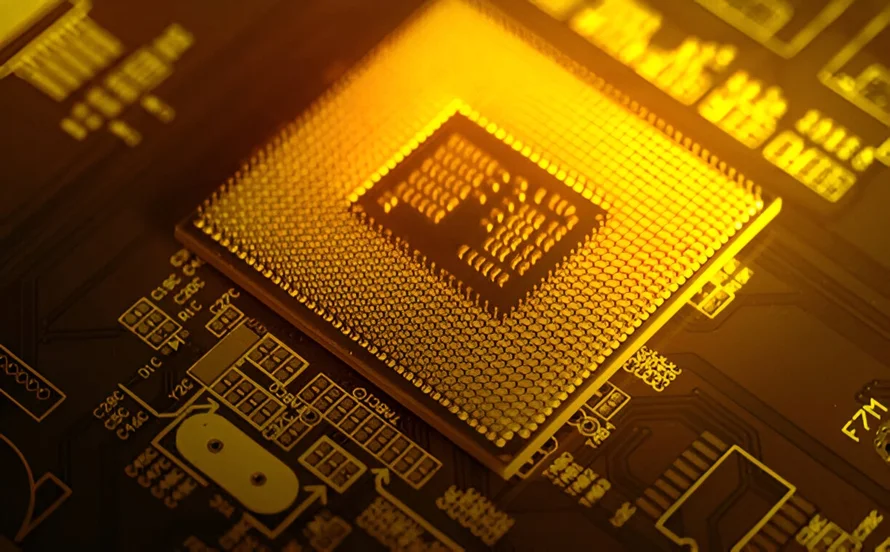

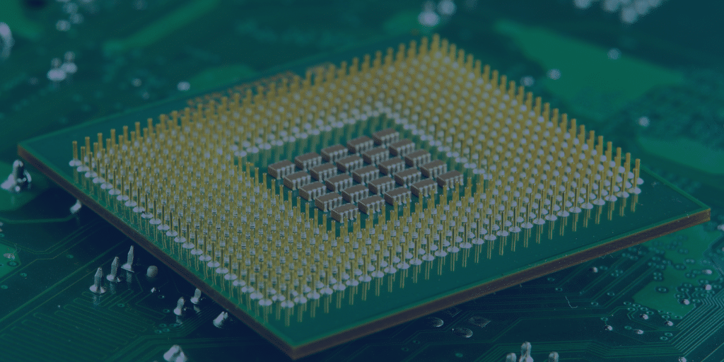

IC substrate provides a connection between the PCB and the IC packages which are built on a Printed Circuit Board. For example, it looks like HDI PCBs with surface mount components.
we provide precision IC Substrate PCB design, fabrication, assembly, and engineering services for advanced semiconductor and high-density electronic applications. IC substrates serve as the critical interface between semiconductor chips and printed circuit boards, enabling superior electrical performance, efficient signal transmission, and enhanced thermal management.
Modern semiconductor devices require highly sophisticated substrate technologies capable of supporting fine-pitch interconnections, high I/O density, and exceptional signal integrity.

Ball Grid Array IC Substrate::Ball grid array IC packages use over 300 pins and high-performance based IC. Most processor types are BGA which tend to heat up more. 2,4,6 Layers (2+2+2 stacked via)
Chip Scale IC Package:The chip-scale substrate IC is thin and it is used for low pin count which is compact. Smaller package is used in memory, Communication, and lightweight commercial products
Single Chip IC Package: It’s a small IC package with a single IC on it like memory devices, telecommunication products or IC packages with a lesser pin count.
Flip Chip IC Substrate:Flip chip substrates are used for the Flip chip and Chip scale substrate IC. This aids in heat dissipation with protection for the circuits and reduces signal interference.
Copper Pattern and Plating:The copper pattern that is required for the circuit is taken and film is deposited on the laminate. The plating of copper happens with high precision using a chemical process.
Solder Mask:The solder mask consists of an IC substrate that is printed by filling the holes that fill on the cap of copper plating. The thickness of the copper plating circuit should be maintained at less than 10 mm for a better and hassle-free process.
Surface Treatment:The most common surface finish is EMIG or ENEPIG of gold alloys for surface finish with proper conductivity and uniform thickness.
Production Test:IC substrate is tested for reliability and internal connectivity with quality inspection in the last stage. Testing methods can include reliable integrated testing with Gigs or End-of-line testers.


As electronic devices continue to become smaller, faster, and more powerful, IC Substrate PCBs play a vital role in enabling next-generation semiconductor packaging technologies. Our advanced engineering, precision fabrication, and comprehensive quality control help customers build high-performance electronic products that meet the evolving demands of modern computing, telecommunications, automotive systems, and industrial electronics.
Find answers to common questions about ultra-fine pitch routing, ABF materials, mSAP manufacturing, and advanced chip packaging solutions.
An IC (Integrated Circuit) Substrate is the highest tier of high-density PCB manufacturing. It acts as the direct physical and electrical bridge between a bare semiconductor chip (the IC die) and the main circuit board. It "fans out" the microscopic nano-scale pins on the chip to the macroscopic millimeter-scale pads on the mainboard.
While advanced HDI boards have fine trace widths (e.g., 2 to 3 mils), IC Substrates operate on an entirely different scale. They feature ultra-fine line and space (L/S) resolutions measured in micrometers (often sub-1 mil, or 10-20µm). Because of this microscopic scale, IC Substrates require highly specialized cleanroom manufacturing environments to prevent particle contamination.
Standard PCBs are made using a "subtractive" process (etching away unwanted copper). For IC substrates, we use mSAP (Modified Semi-Additive Process) or SAP (Semi-Additive Process). Instead of etching, we deposit a microscopic seed layer of copper, apply a pattern, and then actively electroplate copper only where the traces are needed. This prevents the "trapezoidal" trace walls common in etching, allowing for perfectly vertical, ultra-fine traces.
Standard FR-4 is rarely used. Instead, we utilize high-performance resins such as BT (Bismaleimide Triazine) and ABF (Ajinomoto Build-up Film). These specialized materials offer extreme dimensional stability, high glass transition temperatures (Tg), and highly controlled dielectric constants necessary for ultra-fast signal routing between the chip and the board.
The Coefficient of Thermal Expansion (CTE) defines how much a material expands when heated. A bare silicon chip expands very little, while a standard PCB expands significantly. The IC Substrate bridges these two. If the substrate's CTE is not perfectly balanced between the silicon and the mainboard, thermal stress will physically shear and crack the delicate micro-solder bumps during operation.
We fabricate substrates customized for a variety of advanced packaging methods, including BGA (Ball Grid Array), CSP (Chip Scale Package), FC (Flip Chip), and highly complex SiP (System-in-Package) designs where multiple dies and passive components are embedded directly into a single substrate module.
Depending on the specific package requirements and material selection (such as ABF), our advanced lithography and mSAP lines can achieve ultra-fine Line and Space (L/S) resolutions down to 10µm / 10µm. This allows for massive I/O counts required by modern CPUs, GPUs, and baseband processors.
For IC substrates, ENEPIG (Electroless Nickel Electroless Palladium Immersion Gold) is widely considered the gold standard. It provides a highly uniform, ultra-flat surface that completely prevents nickel oxidation, making it exceptionally reliable for both gold wire bonding and direct solder bump attach (Flip Chip).
Mechanical drilling is impossible at this scale. We use precision UV and CO2 laser ablation to vaporize the dielectric material and create micro-vias that are often 50µm in diameter or smaller. These vias are then meticulously copper-plated shut (Via-in-Pad) to create flat landing zones for the semiconductor die.
Testing IC substrates requires state-of-the-art optical and robotic systems. We utilize Automated Optical Inspection (AOI) machines specifically calibrated for micrometer resolutions, alongside specialized ultra-fine-pitch Flying Probe testers equipped with microscopic needles to verify absolute electrical continuity across the entire substrate grid.
Partner with Altest Corporation for your next high-reliability PCB fabrication and turnkey SMT assembly project. Our engineering team is ready to review your gerber files and provide a detailed, competitive estimate.

