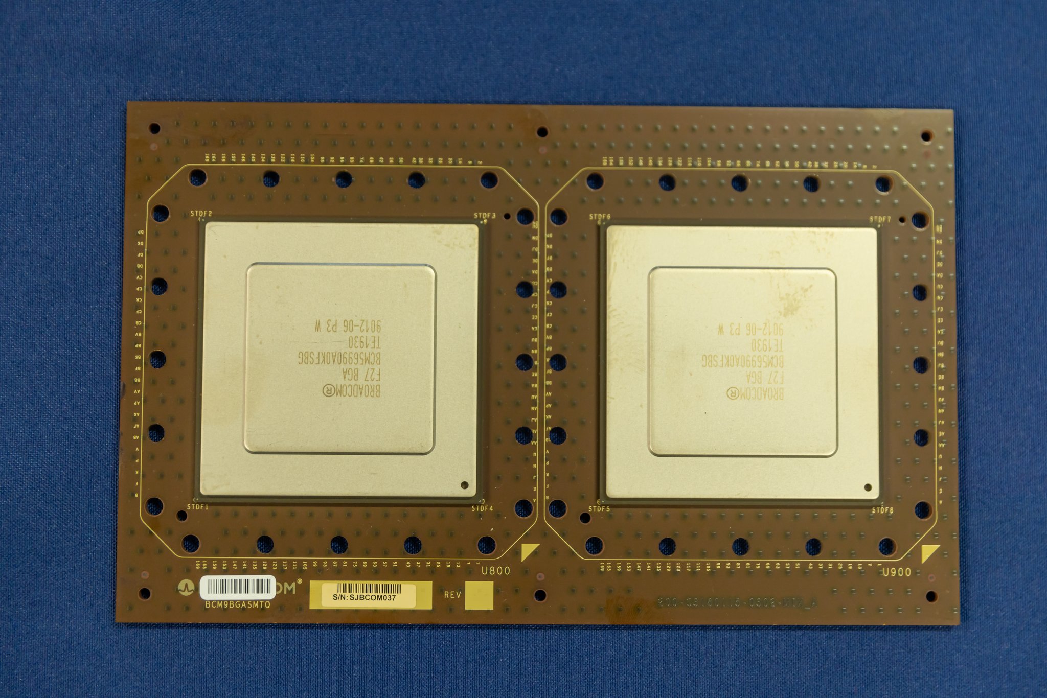

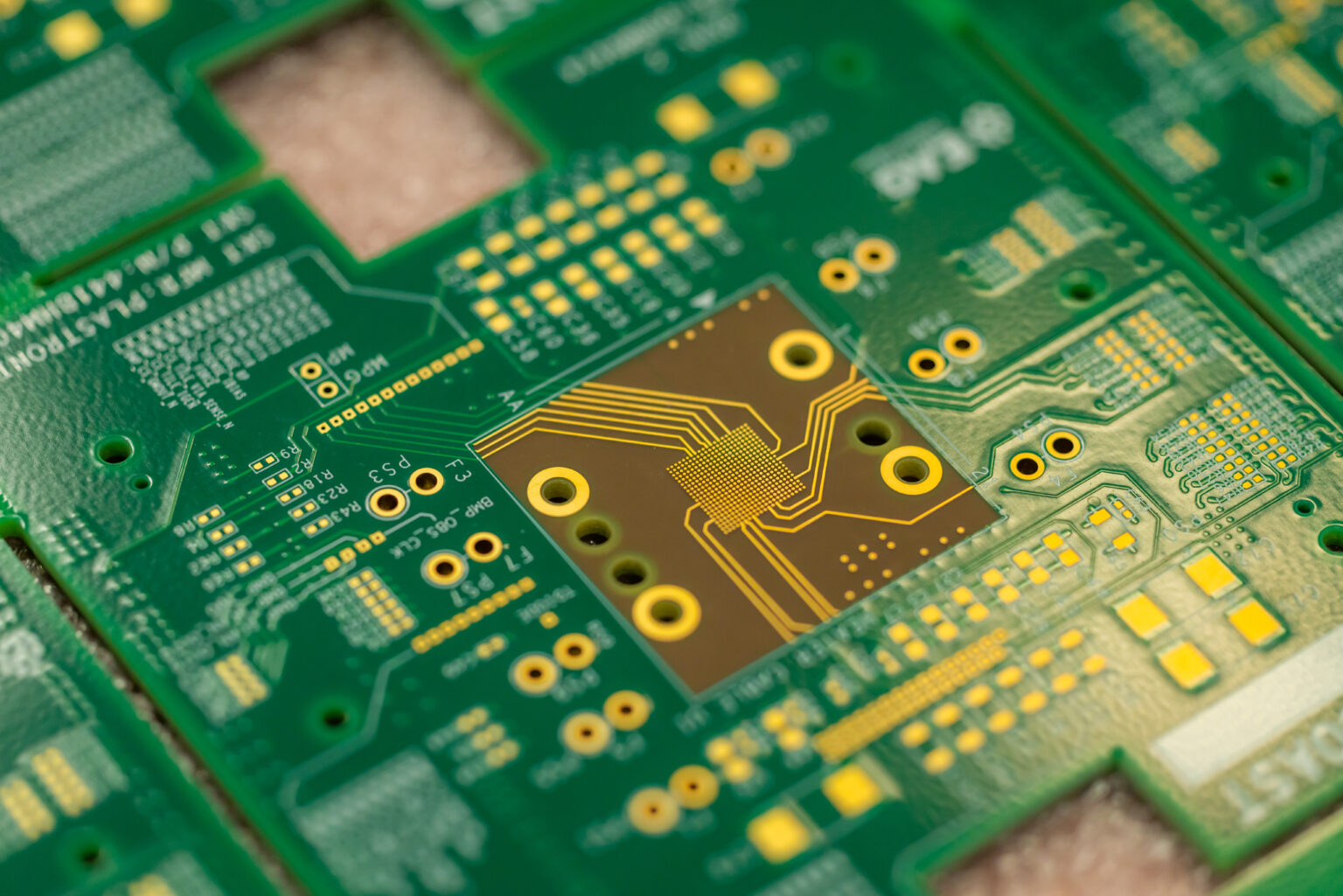

Our Microwave & RF PCB Services are engineered to meet the demanding performance requirements of high-frequency electronic applications. At Altest Corporation, we specialize in the design, fabrication, assembly, and testing of RF and microwave PCBs that deliver exceptional signal integrity, low insertion loss, and precise impedance control. Using advanced materials such as Rogers, PTFE, and other high-frequency laminates, we manufacture reliable circuit boards for aerospace, defense, telecommunications, satellite communications, medical devices, automotive radar, and wireless networking applications.
PCB layout engineering requires careful consideration of several factors to ensure the final board meets performance, manufacturability, and reliability standards.
High-frequency PCB designs require specialized expertise beyond conventional circuit board manufacturing. Our engineering team carefully optimizes controlled impedance, dielectric selection, transmission line design, RF shielding, thermal management, via structures, and signal routing to minimize signal loss, electromagnetic interference (EMI), and crosstalk. Every RF PCB is developed to ensure stable performance, superior reliability, and compliance with the stringent requirements of modern communication and microwave systems.
We manufacture single-layer, multilayer, hybrid, and mixed-material RF PCBs with tight tolerances and rigorous quality control processes. Every board undergoes comprehensive inspection, including Automated Optical Inspection (AOI), X-ray inspection, flying probe testing, impedance verification, and electrical testing, ensuring consistent quality and dependable performance in mission-critical environments. Our end-to-end capabilities also include PCB assembly, Design for Manufacturing (DFM), Design for Test (DFT), and prototype-to-production support.

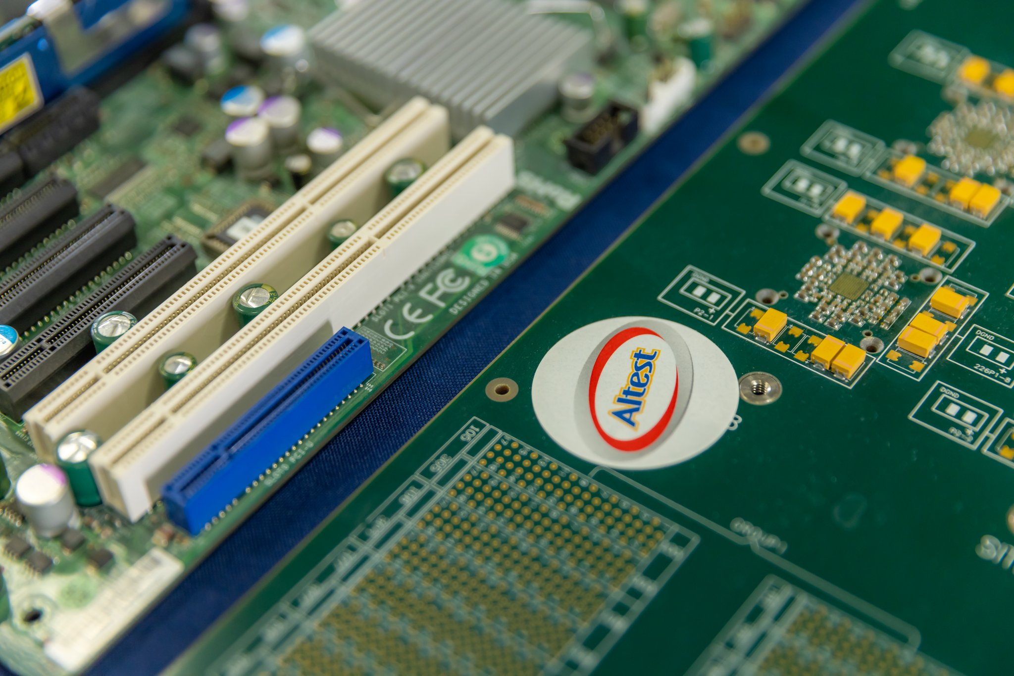
With decades of experience in high-frequency PCB engineering, Altest Corporation delivers reliable solutions for the most demanding RF and microwave applications. Our expertise in advanced PCB materials, precision manufacturing, and high-speed circuit design enables us to produce boards that meet strict industry standards while reducing development time and manufacturing risks. Whether you require prototypes or full-scale production, we provide complete engineering and manufacturing support to help you achieve superior RF performance and long-term product reliability.
Find answers to common questions about high-frequency laminates, impedance control, hybrid stackups, and specialized fabrication techniques for RF applications.
RF (Radio Frequency) and Microwave PCBs are specialized circuit boards designed to operate at extremely high frequencies, typically from 100 MHz to over 100 GHz. Unlike standard digital boards, they require highly stable dielectric materials, ultra-precise etching, and strict impedance control to prevent signal degradation, phase shifts, and electromagnetic interference (EMI).
Standard FR-4 is usually insufficient for microwave applications due to high dielectric loss. We highly recommend advanced, low-loss materials such as Rogers (e.g., RO4000, RO3000 series), Nelco, Taconic, and PTFE (Teflon) based substrates. These materials provide a stable dielectric constant (Dk) and an ultra-low dissipation factor (Df) across wide frequency bands.
We achieve extremely tight impedance control (often +/- 5% or better) by using automated Laser Direct Imaging (LDI) for sub-mil etching accuracy, highly controlled lamination press cycles to ensure uniform dielectric thickness, and predictive software modeling. Every RF batch is verified post-production using Time Domain Reflectometry (TDR) testing.
Yes. To optimize manufacturing costs without sacrificing high-frequency performance, we frequently fabricate hybrid multilayer PCBs. This involves pressing high-cost RF laminates (like Rogers) on the outer signal layers where the RF paths exist, while utilizing standard FR-4 cores for inner power, ground, and low-frequency digital routing layers.
Moisture has a high dielectric constant. If a PCB absorbs moisture, it drastically alters the board's overall Dk, leading to phase shifts, frequency detuning, and signal loss. We utilize ultra-low moisture absorption materials and strict environmental storage controls in our facility to ensure your boards perform reliably in humid or harsh environments.
Surface finish selection is critical to minimize insertion loss. We strongly recommend Electroless Nickel Immersion Gold (ENIG), Immersion Silver, or bare copper with OSP. These finishes provide extremely flat profiles and excellent conductivity without creating a "lossy" barrier that can interfere with the skin effect at microwave frequencies.
RF power amplifiers and continuous-wave microwave components generate substantial localized heat. We integrate heavy copper planes, densely packed thermal via arrays, metal-backed substrates (Aluminum or Copper core), and direct thermal coined inserts to safely pull and dissipate heat away from critical high-power junctions.
At microwave frequencies, electrical current tends to flow only on the extreme outer surface (the "skin") of a copper trace. Rough copper surfaces increase the distance the current must travel, causing resistance and signal loss. We utilize ultra-smooth, low-profile and reverse-treated copper foils to mitigate this effect and preserve absolute signal integrity.
Yes. While PTFE (Teflon) and ceramic-filled materials are notoriously difficult to drill cleanly due to their softness, we employ specialized UV and CO2 laser drilling systems. This allows us to create precise blind, buried, and stacked micro-vias, which are essential for shortening signal paths and eliminating via stub resonance in RF designs.
Absolutely. Our Silicon Valley facility is fully ITAR registered, ISO 9001:2015 certified, and AS9100D certified. We routinely manufacture high-reliability RF and Microwave PCBs that meet stringent military (MIL-PRF-31032) and aerospace quality requirements for satellites, radar, and secure communications.
Partner with Altest Corporation for your next high-reliability PCB fabrication and turnkey SMT assembly project. Our engineering team is ready to review your gerber files and provide a detailed, competitive estimate.

