DFM Check: In this verification check, all layers are verified by the DFM engineer. He verifies all types of errors in the PCB. So, it would be easy for the production floor to make boards without any errors.
Material Selection and Cutting:There are many materials available in the production inventory. So, the material was selected and cut according to the requirements of the order.
Inner Layers Process::At this stage, the inner layer image was transferred to the printed circuit board using UV films and dry films, and then etching was done.
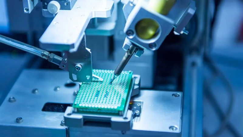
AOI (Automated optical inspection):AOI means automated optical inspection. So, this inspection converts the circuitry image to digital images. Also, AOI inspects the board to ensure it is free from defects. Then the manual visual inspector verifies the inner layers manually.
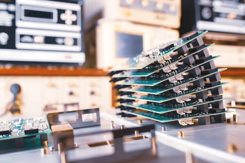
Fabricating multilayer PCBs requires precision engineering and advanced manufacturing expertise. Our facilities utilize high-precision lamination, laser drilling, controlled impedance processing, sequential lamination, blind and buried vias, via-in-pad technology, heavy copper construction, and fine-line imaging to produce complex circuit boards with outstanding accuracy.
Lamination:Lamination is the process of combining or bonding the inner copper foil, core, and prepregs to make solid layers. Lamination machines are set up with some parameters to heat and pressure those inner layers to make a solid layer.
Drilling:Multilayer printed circuit boards have various types of drilling according to the requirements, like blind-buried. So, the drilling machine drills the board as per the given data loaded into the drilling machine.
Copper Plating:PCBs are pulled down in a copper plating bath to add copper plating onto the PCB. It increases the thickness and makes the PCB robust.
Outer Layer Process:This process is the same as the inner layers. However, the inner layers are extended as per requirements, and the outer layers have only two layers, like the top and bottom. Also, the top and bottom layers were done with image transfer and etching. So it would be free for other processes.
At Altest Corporation, we provide advanced Multilayer PCB Fabrication services for industries that require complex, high-density, and high-reliability electronic solutions. Our state-of-the-art manufacturing processes support 4-layer to 40+ layer PCBs, delivering exceptional electrical performance, precise layer alignment, and superior structural integrity. Whether you need rapid prototypes, low-volume production, or high-volume manufacturing, our IPC-compliant fabrication capabilities ensure every multilayer PCB meets the highest standards of quality, reliability, and performance.
With decades of experience in advanced PCB manufacturing, Altest Corporation delivers precision-fabricated multilayer circuit boards for aerospace, defense, medical devices, telecommunications, automotive, industrial automation, semiconductor, and high-performance computing applications. From engineering support and material selection to fabrication, PCB assembly, and final testing, we provide complete turnkey manufacturing solutions under one roof. Our commitment to quality, fast turnaround times, and engineering excellence helps customers accelerate product development while ensuring dependable performance in the most demanding environments.
Find answers to common questions about complex stackups, lamination cycles, inner-layer alignment, and high-density layer routing.
A multi-layer PCB is a printed circuit board comprised of three or more conductive copper layers. These layers are separated by insulating dielectric materials (prepreg and core) and permanently bonded together under extreme heat and pressure to form a single, solid board.
Multi-layer boards are essential for modern, complex electronics. They allow you to pack incredibly high circuit density into a small physical footprint. Furthermore, dedicating specific inner layers entirely to Power and Ground planes drastically improves signal integrity, reduces cross-talk, and provides excellent electromagnetic interference (EMI) shielding.
Our Silicon Valley facility is equipped with advanced lamination presses capable of reliably manufacturing highly complex, high-density multi-layer boards with up to 40 layers. This allows us to support extreme backplane and high-capacity server architectures.
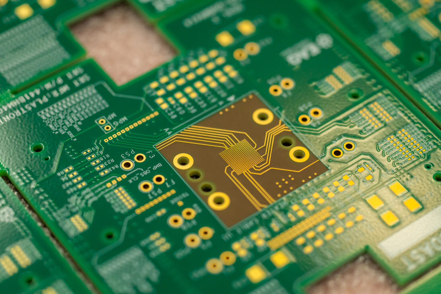
The layer stackup refers to the exact sequential arrangement of copper and insulating dielectric layers. A properly engineered stackup is the foundation of the board's electrical performance. It dictates impedance control, determines thermal dissipation efficiency, and must be symmetrically balanced to prevent the board from warping during manufacturing or SMT reflow.
Layer-to-layer registration is one of the hardest challenges in multi-layer fabrication. We utilize precision optical punching systems to create registration tooling holes on every inner layer. During the layup process, these layers are stacked on steel pins, and we use real-time X-ray inspection to verify micrometer-perfect alignment before the press cycle begins.
We use "Prepreg" (pre-impregnated fiberglass). It is a fiberglass weave coated with a partially cured epoxy resin. During the high-temperature and vacuum-pressure environment of the lamination press, this resin melts, flows to fill all the gaps between the etched copper circuitry, and then permanently hardens to glue the core layers together.
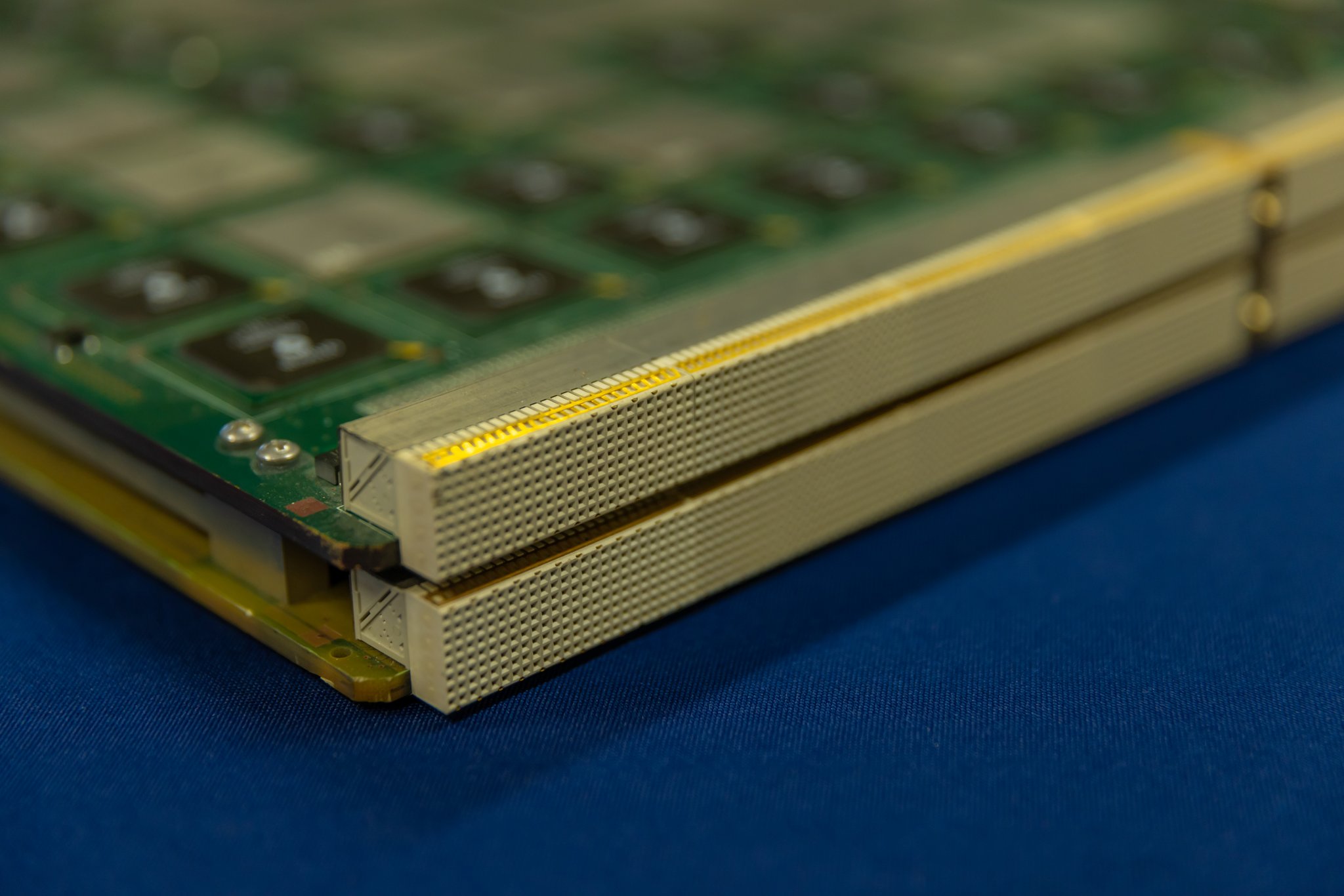
Inter-layer communication is achieved using vias. For multi-layer boards, this includes standard Plated Through-Holes (PTH) that drill through the entire board, as well as advanced routing structures like Blind Vias (connecting an outer layer to an inner layer) and Buried Vias (connecting inner layers completely hidden from the surface).
Standard multi-layer boards are pressed in a single cycle. However, complex HDI boards requiring blind or buried vias demand "Sequential Lamination." This means a subset of the inner layers is pressed, drilled, and plated first, and then additional outer layers are laminated on top of that sub-assembly in a secondary (or tertiary) press cycle.
Before the board is even laminated together, 100% of the inner core layers are scanned using Automated Optical Inspection (AOI) to catch any microscopic shorts or open traces. Once the board is fully laminated and drilled, we use 3D X-Ray and Flying Probe electrical testing to guarantee continuity down the via barrels to the hidden inner pads.
Yes. Every additional core pair requires its own separate imaging, etching, and AOI inspection cycle before lamination can begin. Furthermore, drilling high-layer-count boards requires slower feed rates to maintain accuracy. While it takes longer than a 2-layer board, our optimized USA facility can still produce complex multi-layer prototypes rapidly.
Partner with Altest Corporation for your next high-reliability PCB fabrication and turnkey SMT assembly project. Our engineering team is ready to review your gerber files and provide a detailed, competitive estimate.
