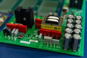
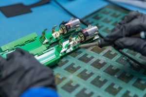
PCBs, the lifeblood of electronic devices, require meticulous fabrication processes. The foundation of every electronic device begins with a well-designed and efficiently manufactured PCB. Engineers often find themselves navigating through a labyrinth of steps, each crucial to the functionality of the final product. Understanding these foundational processes is the first step toward mastering PCB fabrication.
The process starts with substrate preparation, which involves selecting the right material, typically a fiberglass-reinforced epoxy resin. The choice of substrate impacts not only the board’s durability but also its overall cost.
Next comes the intricate process of layering, where conductive and insulating layers are stacked to create the desired circuit patterns. This involves using photoresists and etching techniques that demand precision and expertise. Each layer adds to the complexity and, consequently, the cost.
Lastly, holes are drilled, and vias are plated to establish electrical connections between layers. This step requires specialized equipment and skilled operators, further influencing the manufacturing cost. By grasping these basics, electronics engineers can better appreciate the intricacies involved in PCB fabrication.

Detailed Exploration of Substrate Preparation
Substrate preparation is a critical stage in PCB fabrication that sets the tone for the entire process. The choice of substrate material significantly impacts both the performance and cost of the final product, making it a pivotal decision in PCB manufacturing.
Engineers must choose between various materials, with FR-4 being the most commonly used due to its balance of performance and affordability. However, high-frequency or high-performance applications may require specialized substrates like Rogers or Teflon, which come at a premium cost but offer superior electrical properties.
The preparation process involves cutting the chosen material into panels, ensuring precise dimensions to minimize waste. This initial precision is vital for cost control, as any deviation can lead to material wastage and increased expenses.
Furthermore, the substrate must undergo thorough cleaning to remove contaminants that could impact the adhesion of subsequent layers. Even the smallest impurity can lead to defects in the final product, emphasizing the importance of meticulous substrate preparation.
The Intricacies of Layering and Patterning
Layering and patterning are where the magic of PCB design truly comes to life. This stage involves creating the intricate circuit paths that define the functionality of the board. However, this complexity also introduces significant cost considerations.
Photoresist application is the first step, where a light-sensitive material is applied to the substrate. This resist protects areas of the substrate during etching, allowing for precise patterning of circuit traces. The accuracy of this step directly affects the board’s performance and can impact manufacturing costs.
Etching follows, where unwanted copper is removed to reveal the desired circuit patterns. This step demands precision and control, as over-etching can lead to circuit failure, while under-etching can result in unwanted short circuits. Balancing these factors is essential for cost-effective manufacturing.
Each layer must be carefully aligned during stacking to ensure proper electrical connections and functionality. Misalignment can lead to defects that require costly rework, emphasizing the need for skilled operators and precise equipment.

The Role of Drilling and Via Plating
Drilling and via plating are essential steps in PCB fabrication, establishing the critical connections between layers. Accurate hole drilling is paramount, as even minor deviations can lead to connectivity issues and increased costs.
Drilling machines use computer-controlled systems to achieve precision, minimizing errors and optimizing production efficiency. Engineers must carefully plan the drill pattern to ensure the integrity of the final product.
Via plating follows, where holes are coated with conductive materials to enable electrical connections. This step requires specialized chemicals and equipment, adding to the overall manufacturing cost. Proper via plating ensures signal integrity and reliability, crucial for high-performance applications.
By mastering these steps, electronics engineers can optimize the cost-effectiveness of PCB fabrication while maintaining the desired quality and functionality of the final product.
Material Selection and Its Impact on Costs
Material selection is a fundamental aspect of PCB fabrication that significantly influences both performance and cost. Engineers face a myriad of options, each with distinct characteristics and price points, making this decision a delicate balancing act.
FR-4 remains the go-to choice for many applications due to its affordability and versatility. However, for high-frequency or specialized applications, materials like Rogers or Teflon may be necessary, albeit at a higher cost.
The choice of material also impacts thermal performance, signal integrity, and overall reliability. Engineers must weigh these factors against budget constraints to achieve an optimal balance.

To manage costs effectively, engineers should engage in thorough research and consult material experts to make informed decisions. By considering both performance requirements and budgetary limitations, engineers can select the most cost-effective materials for their specific applications.
Advanced Techniques in PCB Design and Their Cost Implications
Advancements in PCB design have led to the development of innovative techniques that enhance performance but also introduce cost implications. Understanding these techniques is crucial for engineers seeking to optimize both functionality and budget.
High-density interconnect (HDI) technology allows for more components and connections within a smaller footprint, enabling compact designs. However, the increased complexity and precision required for HDI boards result in higher manufacturing costs.
Embedded components, such as resistors and capacitors, eliminate the need for surface mounting, reducing board size and improving performance. Yet, the integration of embedded components adds complexity and cost to the fabrication process.
Flex and rigid-flex PCBs offer design flexibility for applications with unique form factors. While these technologies provide distinct advantages, they require specialized materials and processes, contributing to increased costs.
Engineers must carefully evaluate the benefits and trade-offs of these advanced techniques to ensure they align with project requirements and budget constraints.
Quality Control Measures in PCB Fabrication
Quality control is an integral part of PCB fabrication, ensuring that the final product meets performance and reliability standards. Implementing effective quality control measures is essential for minimizing defects and optimizing cost-effectiveness.
Automated optical inspection (AOI) is a widely used technique that leverages advanced imaging to detect defects early in the fabrication process. By identifying issues before they escalate, AOI helps reduce rework and associated costs.
Electrical testing is another critical measure, verifying the functionality and integrity of the circuits. This step ensures that the PCB meets design specifications and minimizes the risk of failures in the field.
Implementing robust quality control protocols requires an investment in equipment and training but yields significant returns by reducing defects and enhancing overall product quality. Engineers should prioritize quality control measures to achieve cost-effective and reliable PCB fabrication.
Cost-Effective Strategies for PCB Manufacturing
Achieving cost-effective PCB manufacturing requires a strategic approach that considers various factors throughout the fabrication process. Engineers can implement several strategies to optimize costs while maintaining quality.
Design for manufacturability (DFM) is a proactive strategy that involves designing PCBs with manufacturing efficiency in mind. By simplifying designs and minimizing complex features, engineers can reduce production costs and improve yield.
Partnering with experienced and reputable PCB manufacturers is another effective strategy. Experienced manufacturers offer valuable insights into cost-saving opportunities and possess the expertise to deliver high-quality products efficiently.
Volume production can also lead to cost savings, as increasing production quantities often results in economies of scale. Engineers should carefully plan production schedules to leverage these benefits and reduce per-unit costs.
By implementing these strategies, engineers can achieve cost-effective PCB manufacturing without compromising on quality or performance.
Environmental Considerations in PCB Fabrication
Environmental considerations have become increasingly important in PCB fabrication, prompting engineers to adopt sustainable practices that minimize the environmental impact of production processes.
The use of eco-friendly materials is one approach to reducing environmental impact. Engineers can opt for lead-free solder and halogen-free substrates, which contribute to a more sustainable manufacturing process.
Waste reduction initiatives, such as recycling and repurposing materials, further enhance sustainability efforts. Implementing efficient waste management systems helps reduce the carbon footprint of PCB fabrication.
Compliance with environmental regulations is essential for ensuring responsible manufacturing practices. Engineers should stay informed about industry standards and implement measures to meet or exceed regulatory requirements.
By prioritizing environmental considerations, engineers can contribute to a more sustainable and responsible PCB fabrication industry.
The Future of PCB Fabrication and Cost Optimization
The future of PCB fabrication holds exciting possibilities for cost optimization and innovation, driven by advancements in technology and design.
Additive manufacturing, also known as 3D printing, is poised to revolutionize PCB fabrication by enabling rapid prototyping and reducing material waste. This technology offers the potential for cost savings and accelerated production timelines.
Artificial intelligence and machine learning are transforming design processes by automating complex tasks and optimizing layouts for performance and cost. Engineers can leverage these technologies to streamline design workflows and improve manufacturing efficiency.
Nanotechnology is another frontier in PCB fabrication, enabling the development of smaller and more powerful components. While still in its early stages, nanotechnology has the potential to unlock new possibilities for cost-effective and high-performance PCBs.
Staying informed about these emerging trends and technologies is essential for engineers seeking to remain competitive and capitalize on cost optimization opportunities in the evolving landscape of PCB fabrication.
Conclusion
In the intricate realm of electronics engineering, understanding the fabrication steps and related costs of PCBs is paramount to success. From substrate preparation and layering to drilling and quality control, each step plays a vital role in achieving a cost-effective and high-quality final product.
By adopting strategic approaches, considering environmental impacts, and staying abreast of emerging technologies, engineers can optimize PCB manufacturing cost estimation while maintaining quality and performance.
As you continue your journey in electronics engineering, remember that mastering the art of PCB fabrication is a dynamic process that evolves with industry advancements. By leveraging the insights and strategies outlined in this guide, you can confidently navigate the complexities of PCB fabrication and drive innovation in your projects.
