
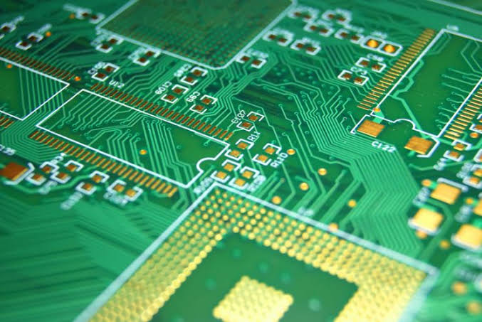
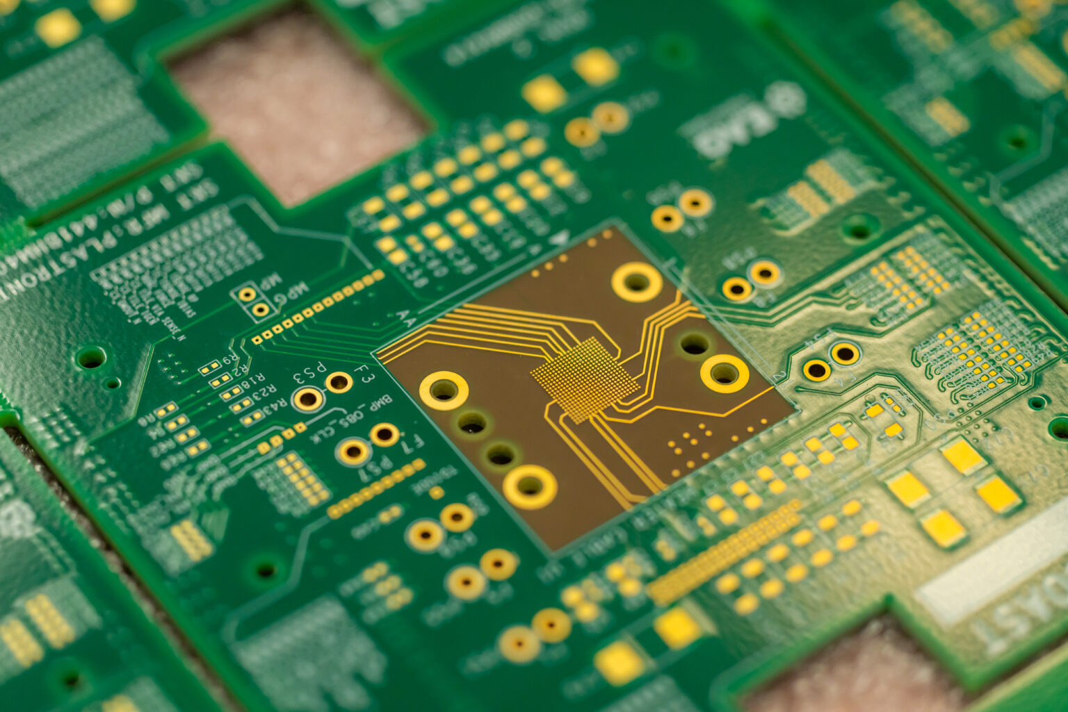
Ensuring Electrical Performance Minimizing Signal Integrity Issues Thermal Management Manufacturability and Cost Efficiency.
Find faster speed-to-revenue with our breadth of technical expertise and product development approach. From FDA-approved medical devices to complex software interfaces, Altest has a proven track record.
PCB layout engineering requires careful consideration of several factors to ensure the final board meets performance, manufacturability, and reliability standards.
.jpg)
Functionality: Components should be placed in a way that aligns with the signal flow, allowing for efficient routing and minimizing the distance between related components.
Accessibility: Components that need regular maintenance or testing should be easy to access on the board.
Components that generate heat, such as power transistors or voltage regulators, should be placed in areas with sufficient space or near heat sinks to ensure proper heat dissipation.
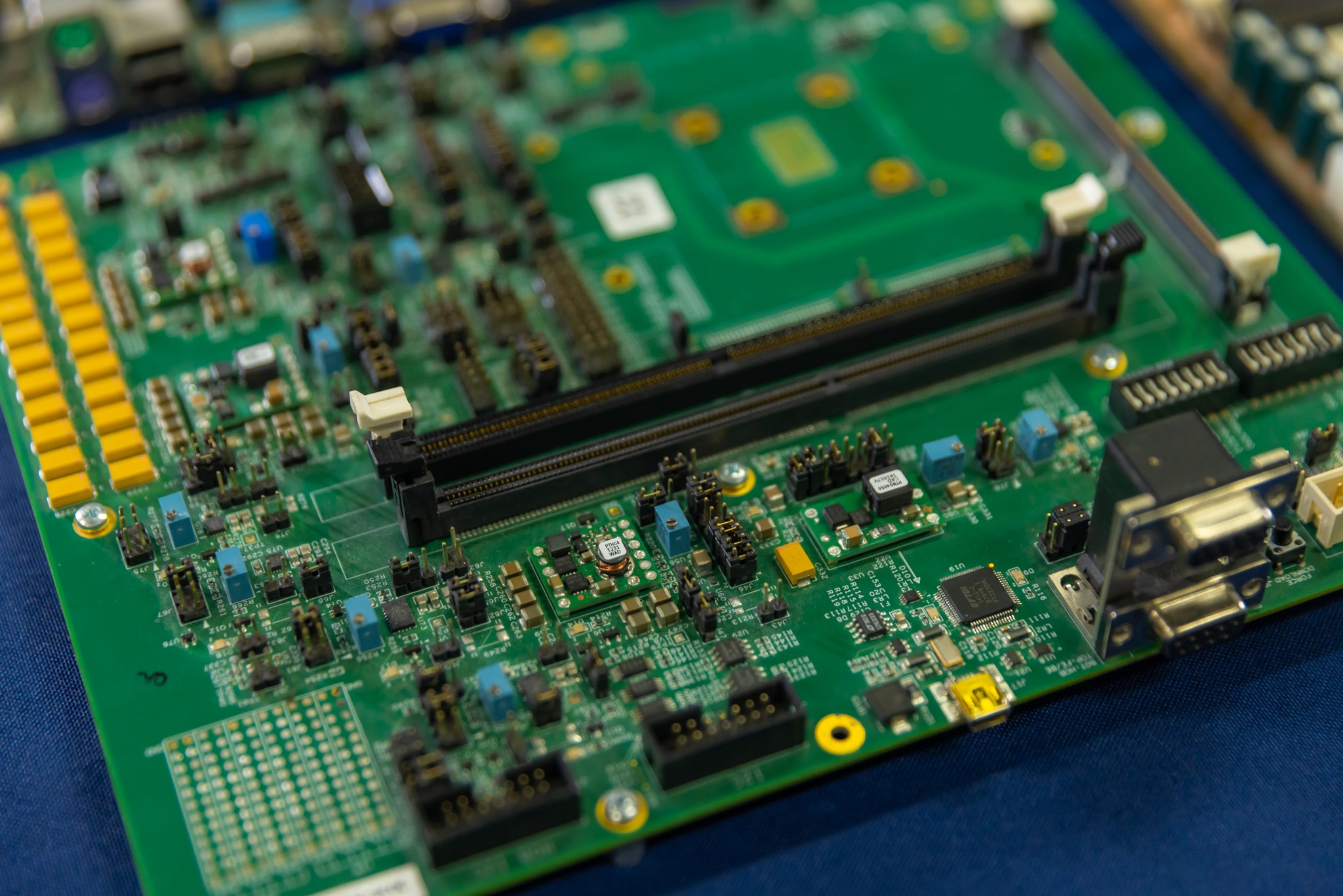
Signal Traces: Signal traces should be as short and direct as possible to minimize resistance, inductance, and capacitance.
Trace Width and Spacing: Proper trace width and spacing are critical for both electrical performance and manufacturability to avoid short circuits.
Find answers to common questions about our CAD software platforms, high-speed routing, HDI design, and DFM integration.
PCB layout is the critical engineering process of translating a logical schematic diagram into a physical printed circuit board design. It involves placing component footprints within strict mechanical boundaries and routing the physical electrical connections (copper traces) to ensure optimal signal integrity and manufacturability.
Our engineering team is highly proficient in industry-leading design tools, including Altium Designer, Cadence Allegro, and Mentor Graphics PADS. This ensures seamless integration with your native files and allows us to accommodate your specific database requirements.
To begin a layout, we typically require a verified schematic (netlist), a preliminary Bill of Materials (BOM), mechanical constraints (DXF/STEP files of your enclosure), and a document detailing any specific routing guidelines, stackup preferences, or impedance requirements.
Yes. Because our layout engineers work alongside our fabrication and assembly teams, DFM and DFT (Design for Testing) principles are applied continuously. We also utilize Siemens Valor NPI software to verify manufacturability before generating final Gerber files, preventing costly revision spins.
Absolutely. We specialize in high-speed digital routing. We carefully manage differential pairs, trace length matching, phase tuning, and strict impedance control to prevent signal reflection and degradation on fast data buses (like PCIe, DDR, and USB 3.0).
Yes. We routinely design complex HDI boards requiring blind and buried vias, stacked/staggered laser micro-vias, and via-in-pad (VIPPO) technology. This expertise is critical for fanning out ultra-fine pitch BGAs and dense component packaging used in modern electronics.
Yes, our engineers are highly experienced in isolating sensitive analog and RF pathways from noisy digital signals. We implement specialized shielding, via stitching, co-planar waveguides, and help select optimal low-loss dielectric materials (like Rogers) for high-frequency performance.
Yes. We handle complex 3D spatial layouts for flex and rigid-flex circuits. We strictly adhere to flex routing rules, ensuring proper bend radiuses, staggered traces across flex zones, and mechanical reliability for both dynamic and static flex applications.
The timeline depends entirely on the board's complexity, pin count, and routing constraints. A simple 2-layer board might take a few days, while a highly dense, 24-layer HDI board could take several weeks. We will provide a detailed, accurate schedule during the initial quoting phase.
You do. Upon completion and final sign-off, Altest Corporation transfers full ownership of all native CAD files, generated Gerbers, ODB++ packages, assembly drawings, and documentation directly back to your team.
Partner with Altest Corporation for your next high-reliability PCB fabrication and turnkey SMT assembly project. Our engineering team is ready to review your gerber files and provide a detailed, competitive estimate.

