
Admin, November 15,2021
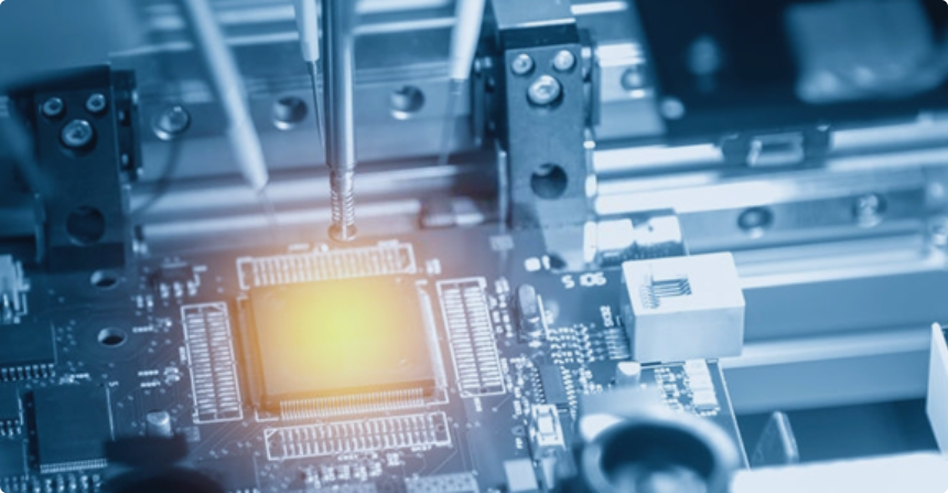
THE PRINT CIRCUIT BOARD ASSEMBLY PROCESS
Altest has always focused on providing a solution in-house to any PCBA challenges that our clients may face. Clients in the past have tasked Altest with fully taking their project from a prototype to a market-ready product through a
PCBA is short for Printed Circuit Board Assembly which is the process of combining electronic components and accessories onto blank printed circuit boards (PCB). To create electronic devices the PCB must be fabricated and then components must be added. PCBs have conductive pathways engraved onto the boards which deliver electricity to the components to operate. Assembling these boards can present unique challenges due to the varying complexities of design and the size of the boards. Different products have vastly different sizes and the capabilities of an assembly firm are dependent on what machines they have and how they set up their assembly lines. Depending on the assembling company they may not be able to manufacture large boards exceeding certain dimensions and thickness due to the machines they have. This article will touch upon the basics of the assembly process from the equipment and tools we use to the types of techniques we use.
Prior to performing any of the above steps, box-build / electro-mechanical assembly manufacturers must acquire certain pieces of information to ensure they build the assembly correctly. The most important pieces of information are the bill of materials (BOM), drawings, and schematics. Additional documents, including wire run lists, test protocols, and sample units, help ensure creating a quality product.
You can learn more about Altest’s equipment and capabilities here.
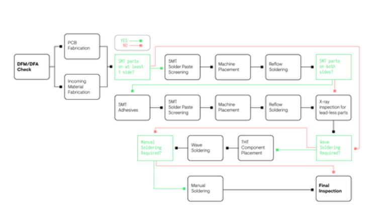
PCBA Process Flow Chart
It all begins with a design for the board itself. Clients usually have a team of in house engineers that design the boards, but if a design is too difficult or they lack an experienced engineering team they can utilize the engineers at the assembly company. Altest has a dedicated team of engineers that are able to assist during this stage of the process. Depending on the assembly company clients can order a fabricated board through them as well.
The assembly process begins with a design for manufacturing check (DFM) which validates a board design based on the manufacturer’s guidelines. A DFM check reviews a client’s designs, part spacing, pin indications, footprint corroboration, and a BOM verification just to name a few techniques Altest uses. This ensures initial errors will be caught early which will prevent delays and RMAs. Altest offers a free DFM check to ensure that a client’s project is complete on time.
A BOM check is done to provide the client with an accurate cost of materials for their project. Once we determine the validity of the BOM the next step is component procurement. Altest has a dedicated parts warehouse where components will be pulled before using third party components. Parts we order for the project are subject to our incoming material inspection check. This ensures that new parts added to our warehouse and to the project kit meet our standards and to ensure any problems will be caught before being assembled. Due to scarcity for certain parts, this may lead to longer lead times and may delay the project. In that scenario, our component engineer will assist in finding a possible alternative component that will work just as fine and speed up lead times.
Everything starts by submitting a quote using our free quote tool here.
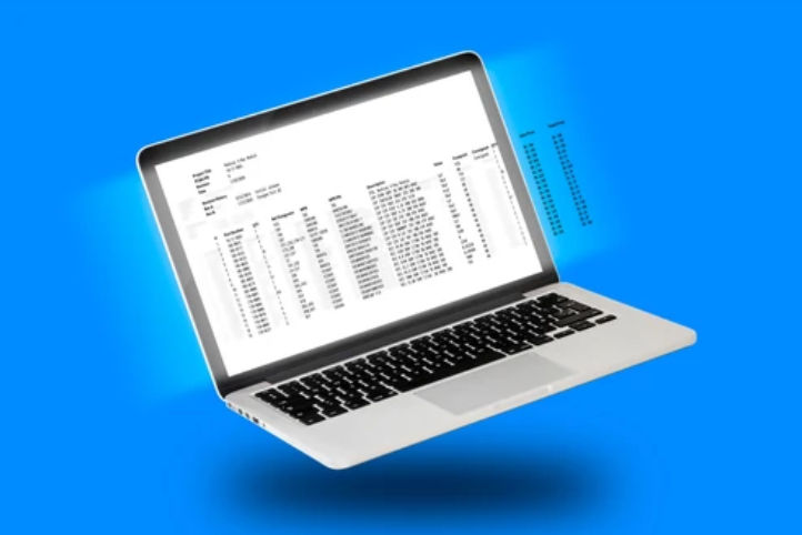
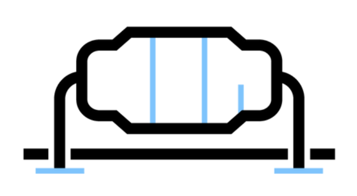
BOM (Bill of Materials)
There are multiple ways to assemble a PCB board. Depending on the design a board can utilize multiple techniques. Different techniques serve different purposes and can significantly impact the cost to manufacture a board. The most used form of manufacturing today, however, is a technique known as surface mounting (SMT).
Surface Mount Technology (SMT): Components are assembled by a technique called soldering. Metal pins on the components allow for easy connection to the PCB board. This technique is the most commonly used form of assembly due to speed, cost, and flexibility. Components can be assembled with higher densities and rapidly with machines. The SMT process allows for components to be mounted on both sides of the board which allows for much more complex designs on the client’s end. SMT machines can place components in the tens of thousands every hour onto PCBs.
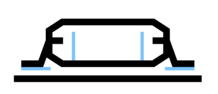
SMT ( Surface Mount Technology) Figure
Through-Hole Mounting (THM): This method involves drilling a hole into the PCB to attach components. Some components and electrical accessories can only be attached using this method such as input connectors. This method adds extra cost and manufacturing time to the project. Through-hole mounting is rarely used if a component can be assembled through the SMT method due to THM taking up more space and limiting design complexity while increasing cost and time to manufacture. However, if a project requires constant insertions or environmental stress then THM would be a good method to ensure longevity.
Through Hole Mount Figure
Electro-mechanical assembly: This method also known as a box-build assembly is the process of using things like custom metalwork, cable assembly, plastics, and harnesses to assemble printed circuit boards with electronic components. Some firms will elect to ship straight to the consumer when the product is made in the manufacturing facility to save on time. Altest offers this as well as RMA support staff as well as warehousing.
Box Build Assembly
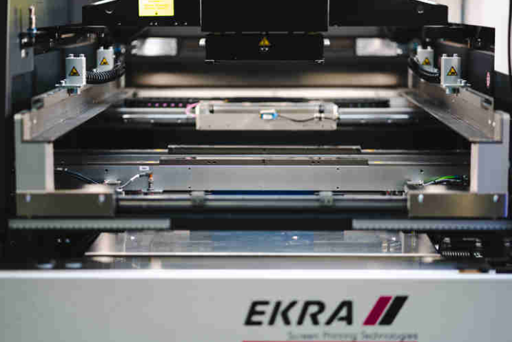
First, a stencil is made that allows for only the pads of the board to be in contact with the solder paste. The screen printer that applies an even coat of the paste onto the board to allow for components to be attached. Altest uses multiple high-speed EKRA and GKG screen printers that allow for large board sizes with high reliability.
Once the board has the solder paste applied to it, it then moves on to a 3D solder paste inspection (SPI) machine. This machine ensures that the correct specified thickness and amount of solder paste was added to the correct areas of the board as per the engineer’s design. This saves time down the assembly process line.
Ekra Screen Printer
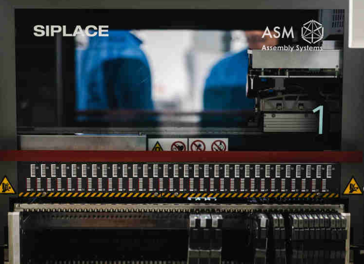
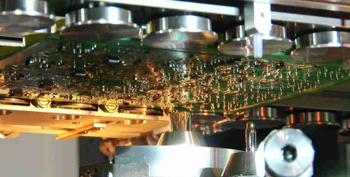
Once the solder paste on the board has been inspected we move onto machine placement of the components otherwise known as pick and place. Just like our screen printing process, Altest has multiple pick and place machines by MyData and ASM that allow us to efficiently manufacture high and low volume projects of varying sizes and complexities without impacting other projects. These pick and place machines vary in speed and capabilities so we made sure to utilize multiple machines to ensure flexibility.
Components are placed onto the board as much as tens of thousands of components an hour. This entire process is completely automated which ensures human error isn’t a factor. These machines are highly precise in their movements down to the millimeter.
SMT Pick and Place Machine
Once the boards have all the necessary components placed the next step would be the reflow oven. The reflow oven applies intense heat to the board which creates a permanent solder joint between the board and component. Some components can’t withstand the heat that the reflow oven puts out so they must be hand soldered.
Some parts require wave soldering to be down. We use a machine here at Altest called a selective soldering machine as well as traditional wave soldering machines. Altest has an in house nitrogen facility that produces the necessary chemicals for wave soldering. This process is used to ensure that heat-sensitive components are not damaged or for through-hole components to be assembled.
Once this step is completed the board will go through a wash containing ionized water which will clean flux residues off. This ensures the board will perform reliably and have longevity. During this process, the board will also undergo a quick manual inspection before moving onto the next step.
Selective Solder Machine
A 3D AOI or automated optical inspection allows us to inspect a PCB after the reflow process. This machine can inspect double-sided boards to ensure we catch any defects that may have been missed throughout the entire process.
Our next inspection machine is an X-Ray machine that can perform non-destructive inspections on optically hidden features of the board such as joint quality confirmation and analysis; component shorts, voiding, opens and more; and other possible issues undetectable by all other inspection processes.
Our next inspection machine is an X-Ray machine that can perform non-destructive inspections on optically hidden features of the board such as joint quality confirmation and analysis; component shorts, voiding, opens and more; and other possible issues undetectable by all other inspection processes.
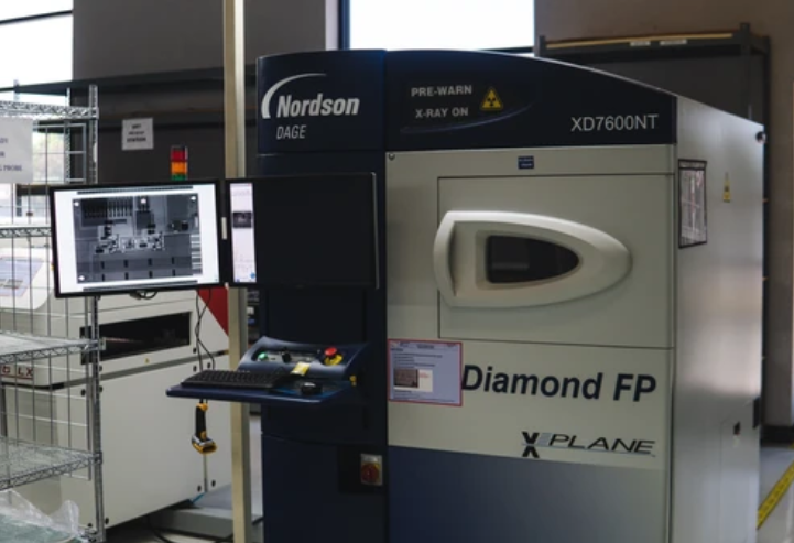
X-Ray Machine
There are multiple forms of testing done to ensure that a PCB functions perfectly. Flying probe testers also referred to as fixture-less in-circuit tests (FICT) are the ideal testing machines for a majority of projects. The board design is uploaded to the machine and the multi probes will “fly” around and test the components on the board. These machines are extremely flexible and allow for the testing of large boards as well as double-sided designs fairly quickly.
There are also functional tests that involve monitoring and debugging the board manually after assembly. Clients may provide our team with testing programs and software that can be tested by our staff before being shipped out.
You can learn more about the testing equipment and processes that we use here.
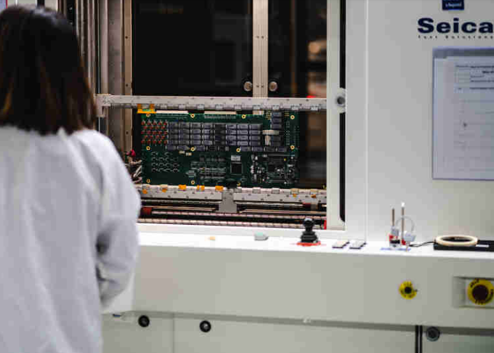
Flying Probe Tester
Once the board has come off the testing process line it is then taken to a final hand inspection. Once our final QC expert gives the green light on the board and ensures that each quality check stamp has been applied for each stage of assembly it is then sent to shipping. Our shipping team then cleans up each board to be sent out to the customer. Each board is carefully cleaned and inspected to ensure the optimal final product for our customer. Our shipping team then packages each board carefully following ESD (electric static discharge) guidelines and shipping safety packaging to ensure nothing damages the boards in transit. Once our customers have received the boards we still stay in close contact to ensure that there are no problems after shipping and if there are any changes that need to be in following iterations.
We at Altest would love to get you jump started on your PCB project. You can book a tour or submit a quote using our free quoting tool and we’ll get back to you on the same day.
Share: