In the evolving world of electronics, through-hole technology remains a staple for robust and durable printed circuit board (PCB) designs. Understanding the rules for through-hole assembly design not only ensures the efficiency of your manufacturing processes but also enhances the reliability and longevity of your products. Whether you’re a manufacturing professional, a PCB designer, or an electrical engineer, mastering these rules is crucial for delivering high-quality electronic devices.
This comprehensive guide will walk you through the essential rules of through-hole assembly design, offering practical tips and insights along the way. By the end of this post, you’ll have a clear understanding of how to optimize your PCB designs for through-hole assembly, ensuring both performance and manufacturability.
The Basics of Through-Hole Technology
What is Through-Hole Technology?
Through-hole technology (THT) involves mounting electronic components on a PCB by inserting their leads through pre-drilled holes and soldering them on the opposite side. This method provides strong mechanical bonds, making it ideal for applications requiring durability and reliability.
Why Choose Through-Hole Over Surface Mount?
While surface mount technology (SMT) is popular for its compactness and efficiency, THT offers superior mechanical strength. It’s especially advantageous in high-stress environments, such as aerospace and automotive industries, where components must withstand significant physical forces.
Key Components in Through-Hole Assembly
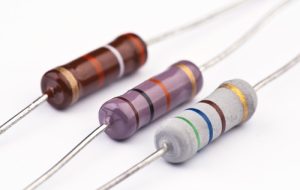
Through-hole assemblies typically include components like resistors, capacitors, inductors, diodes, and larger components like transformers and connectors. These components are chosen for their ability to handle higher power levels and offer more reliable connections than their SMT counterparts.

Design Considerations for Through-Hole Assembly
Hole Size and Tolerance
The size and tolerance of the holes in your PCB are critical. The holes must be large enough to accommodate component leads but not so large that they compromise the mechanical stability of the connection. Typically, a lead-to-hole clearance of 0.2 to 0.3 mm is recommended.
Pad Size and Annular Ring
The pad size and annular ring are equally important. The annular ring is the area of the pad surrounding the hole, and it must be sufficient to ensure a strong solder joint. A minimum annular ring of 0.15 mm is generally advised.
Component Lead Length
The length of the component leads should be optimized for ease of insertion and effective soldering. Leads that are too long can cause soldering issues, while leads that are too short may not penetrate the board adequately, leading to weak joints.
Soldering Techniques for Through-Hole Assembly
Wave Soldering
Wave soldering is a popular technique for through-hole assembly. In this process, the PCB passes over a wave of molten solder, which adheres to the exposed metal areas, creating secure solder joints. This method is efficient for mass production.
Hand Soldering
Hand soldering is often used for small batches or complex assemblies where precision is required. This technique allows for meticulous control but is time-consuming and requires skilled operators.
Selective Soldering
Selective soldering combines the benefits of wave and hand soldering. It uses a programmed nozzle to apply solder to specific areas, making it ideal for mixed-technology boards where some components are surface-mounted.
Ensuring Signal Integrity
Minimizing Inductance and Capacitance
Maintaining signal integrity is crucial in PCB design. To minimize inductance and capacitance, keep the leads short and the traces direct. This approach reduces the potential for signal degradation and electromagnetic interference.
Grounding and Shielding
Proper grounding and shielding practices are essential to prevent noise and interference. Use ground planes and shielding techniques to protect sensitive signals, ensuring reliable performance even in noisy environments.
Thermal Management
Effective thermal management is vital to prevent overheating and ensure component longevity. Incorporate thermal vias and heat sinks to dissipate heat efficiently, especially for high-power components.
Testing and Inspection
Visual Inspection
Visual inspection is the first line of defense in quality control. Inspect the solder joints and component placement to identify any obvious defects, such as cold joints or misaligned components.
Automated Optical Inspection (AOI)
AOI systems use cameras to automatically inspect PCBs for defects. This method is faster and more reliable than manual inspection, making it ideal for high-volume production.
In-Circuit Testing (ICT)
ICT involves using test probes to check the electrical performance of the assembled PCB. This method verifies that all components are correctly placed and functioning as intended, ensuring the board meets design specifications.
Common Pitfalls in Through-Hole Assembly Design
Inadequate Hole Size
One common mistake is using holes that are either too small or too large. This can lead to poor solder joints and unreliable connections. Always double-check your hole sizes and tolerances against component lead specifications.
Poor Solder Joint Quality
Poor solder joint quality can result from insufficient solder, improper heating, or contamination. Ensure your soldering processes are well-controlled and regularly maintained to prevent these issues.
Misaligned Components
Misaligned components can cause functional failures and complicate assembly processes. Use fiducials and alignment aids to ensure precise component placement during assembly.
Best Practices for Design for Manufacturing (DFM)
Collaborate with Your Manufacturer
Collaboration with your manufacturer during the design phase can identify potential issues early and streamline production. Your manufacturer can provide valuable insights into manufacturability and suggest design improvements.
Standardize Component Placement
Standardizing component placement simplifies assembly and reduces the risk of errors. Group similar components together and orient them consistently to facilitate efficient soldering and inspection.
Optimize Panelization
Panelization involves arranging multiple PCBs on a single panel for simultaneous processing. Optimizing panelization can reduce waste, lower costs, and improve throughput. Work with your manufacturer to determine the best panel layout for your design.
Future Trends in Through-Hole Technology
Hybrid Assemblies
Hybrid assemblies that combine THT and SMT components are becoming more common. This approach leverages the strengths of both technologies to create highly reliable and compact designs.
Advanced Materials
New materials, such as high-temperature laminates and advanced solder alloys, are being developed to enhance the performance and reliability of through-hole assemblies. Staying informed about these advancements can give you a competitive edge.
Automation and AI
Automation and artificial intelligence are transforming PCB assembly processes. Automated systems can handle complex assemblies with high precision, while AI algorithms optimize design and production workflows for maximum efficiency.
Conclusion
Through-hole assembly design remains a critical skill for manufacturing professionals, PCB designers, and electrical engineers. By adhering to the rules and best practices outlined in this guide, you can create robust, reliable, and efficient PCB designs that stand the test of time.
Remember, the key to success lies in attention to detail, collaboration with your manufacturer, and staying abreast of industry trends. For further assistance and expert advice, consider reaching out to our team of specialists who can help you refine your designs and achieve excellence in your through-hole assembly projects.
Start optimizing your through-hole assembly design today and experience the difference it can make in your product’s performance and reliability.
