.png)
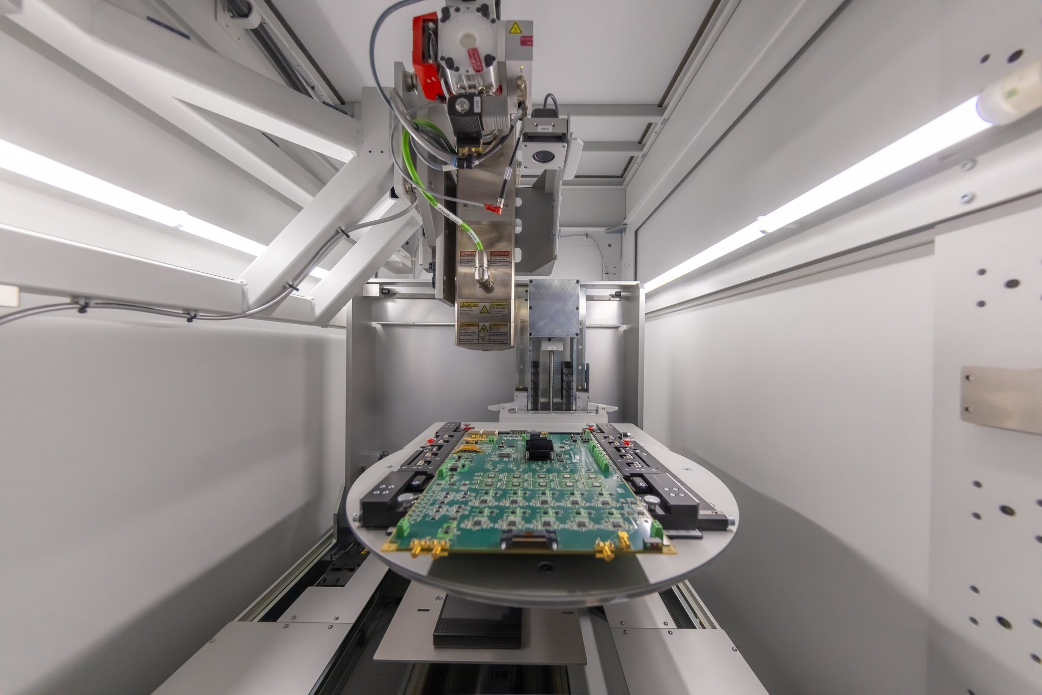
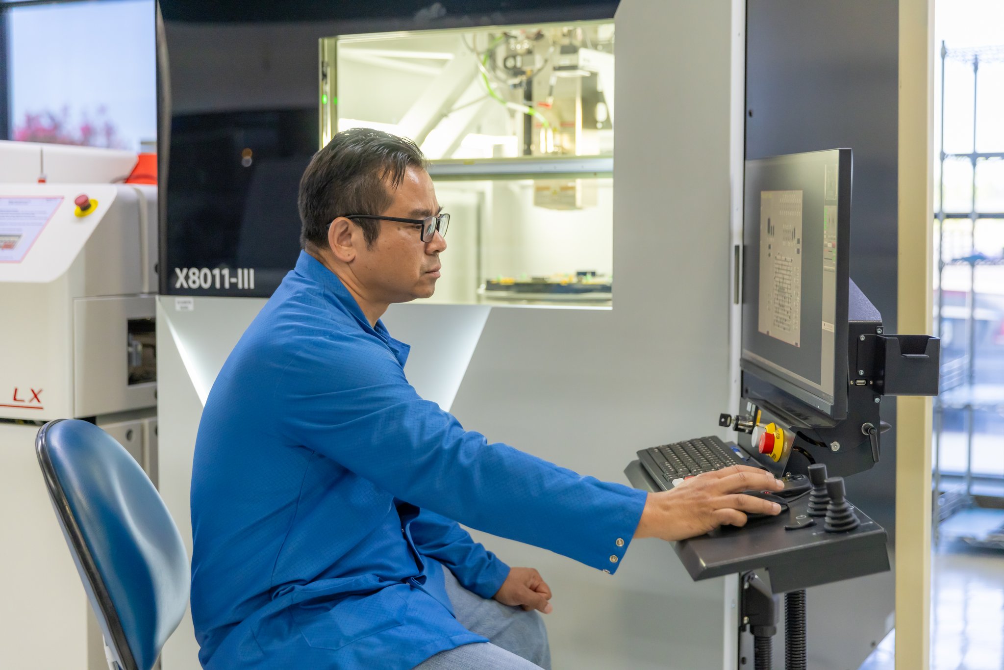
At Altest Corporation, our 3D X-Ray Inspection (AXI) services provide non-destructive inspection (NDI) of complex printed circuit board assemblies where conventional optical inspection cannot detect hidden solder joint defects. Utilizing high-resolution Computed Tomography (CT) and 3D Automated X-Ray Inspection (AXI) technology, we perform volumetric analysis of solder joints, internal PCB structures, plated through-holes, vias, and concealed interconnections with micron-level accuracy. Our inspection process ensures compliance with IPC-A-610, IPC-7095, IPC-6012, and IPC-2221 quality standards while delivering superior defect detection for mission-critical electronic assemblies.
Our 3D AXI systems provide quantitative measurements that support advanced manufacturing process control and failure analysis.
.jpg)
DAGE X-RAY:DAGE X-RAY system with 3D reconstruction.
CT-Computed Tomography :Very High Power CT (Computed Tomography X-Ray to see under BGA’s).
X-Ray detection :Very High Power CT (Computed Tomography X-Ray to see under BGA’s) The system has geometric magnification and total 60,000x with digital zoom. There is nothing that you cannot see in the process of X-Ray detection. Altest X-Ray System is used to inspect circuit boards and Semiconductor devices too detect errors/anomolies in the PCB assembly.
High-Resolution 3D Computed Tomography (CT):Non-destructive volumetric imaging of hidden solder joints, internal PCB layers, vias, and semiconductor packages.
Advanced Defect Detection:Identifies voiding, Head-in-Pillow (HIP), non-wet opens, solder bridging, barrel fill defects, cracked vias, delamination, and internal structural anomalies.
Quantitative Process Analysis:Measures solder volume, ball collapse, void percentage, component alignment, layer registration, and thermal pad coverage for process optimization.
IPC-Compliant Inspection & Traceability:Supports IPC-A-610, IPC-7095, IPC-6012, and customer-specific acceptance criteria with complete inspection documentation.
.jpg)
.jpg)
With decades of experience in advanced PCB manufacturing, assembly, and inspection, Altest Corporation combines state-of-the-art 3D AXI technology, IPC-certified quality systems, and experienced reliability engineers to provide world-class inspection services. Our inspection laboratory supports rapid prototype validation, process qualification, production quality assurance, and comprehensive failure analysis with fast turnaround and complete traceability
Find answers to common questions about automated X-ray inspection (AXI), hidden defect detection, BGA joint validation, and volumetric void analysis.
3D Automated X-Ray Inspection (AXI) is a non-destructive testing method that uses X-ray imaging combined with computed tomography (CT) or laminography to create highly detailed, 3D cross-sectional slices of a printed circuit board. This technology allows quality engineers to inspect the structural integrity of solder joints that are hidden completely from view.
Traditional 2D X-ray creates a flat, top-down image. On double-sided boards, components on the top and bottom overlap, creating confusing shadows that make it difficult to isolate faults. 3D X-ray captures multiple angled images and reconstructs geometric slices, allowing us to isolate specific layers and inspect complex assemblies without overlapping interference.
All solder connections on a Ball Grid Array (BGA) or Quad Flat No-Lead (QFN) component are located entirely underneath the package. Because they are physically hidden, it is impossible to verify them using standard optical cameras or human inspection. X-ray is the only non-destructive way to guarantee these connections are solid and free of shorts.
Our 3D AXI systems excel at finding issues that escape visible inspection, including solder voids, bridging (shorts) between hidden pins, missing solder balls, insufficient wetting, open connections, and complex "head-in-pillow" (HiP) defects on advanced surface mount packages.
Voiding occurs when flux gas bubbles get trapped inside the molten solder during the reflow process. While minor voiding is common, excessive voiding weakens both the mechanical and thermal integrity of the joint. 3D AXI automatically calculates the exact volumetric percentage of voids, ensuring it complies with strict IPC standards (typically keeping voids under 25-30%).
HiP is a notorious hidden defect where a BGA solder ball rests in the solder paste but fails to fully coalesce and form a true metallurgical bond—resembling a head resting on a pillow. It often passes initial electrical testing but fails in the field due to mechanical stress. 3D X-Ray provides the distinct slice-level detail needed to detect this separation line.
Yes. For high-reliability and IPC Class III applications, it is crucial to verify that the solder has properly flowed completely through the plated barrel. 3D X-ray can accurately measure the volumetric barrel fill percentage (verifying it meets the required 75%+ standard) without having to physically cut the board open for microsectioning.
They are complementary technologies. AOI uses visible light cameras to check for surface-level defects like missing parts, skewed placement, and the visual quality of exposed solder fillets. AXI uses radiation to penetrate the physical materials, allowing us to inspect the internal geometry, thickness, and hidden structural integrity of the joints beneath the surface.
Generally, no. While massive doses of radiation can affect sensitive components like specialized memory chips or image sensors, our automated 3D AXI systems are programmed with optimized exposure times and controlled energy levels (kV/µA). This provides high-resolution imaging while remaining well within the safe dosage limits for standard electronics.
This depends entirely on your project's compliance requirements. For mission-critical aerospace, medical, or defense boards, 100% AXI inspection is often mandatory. For standard commercial electronics, we typically perform 3D AXI on "first-article" boards to validate the oven reflow profile, followed by strict statistical batch sampling during volume production.
Partner with Altest Corporation for your next high-reliability PCB fabrication and turnkey SMT assembly project. Our engineering team is ready to review your gerber files and provide a detailed, competitive estimate.

