
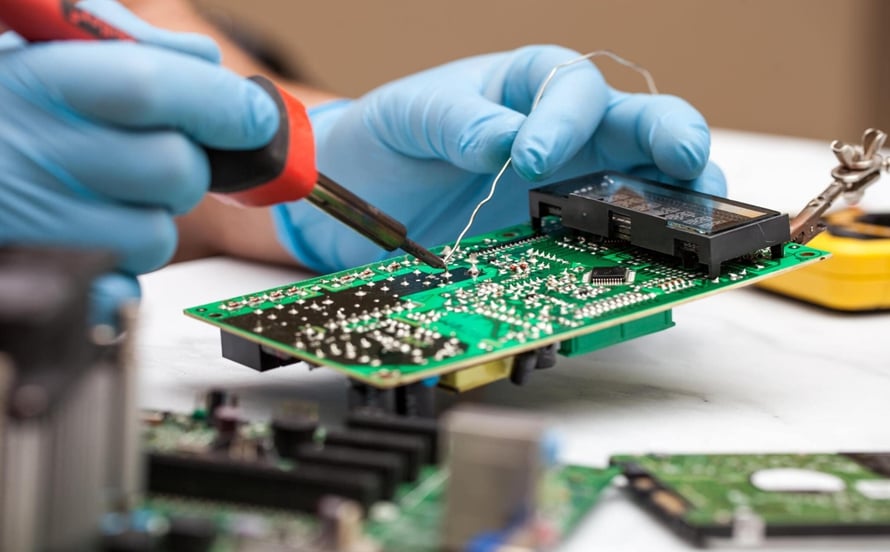
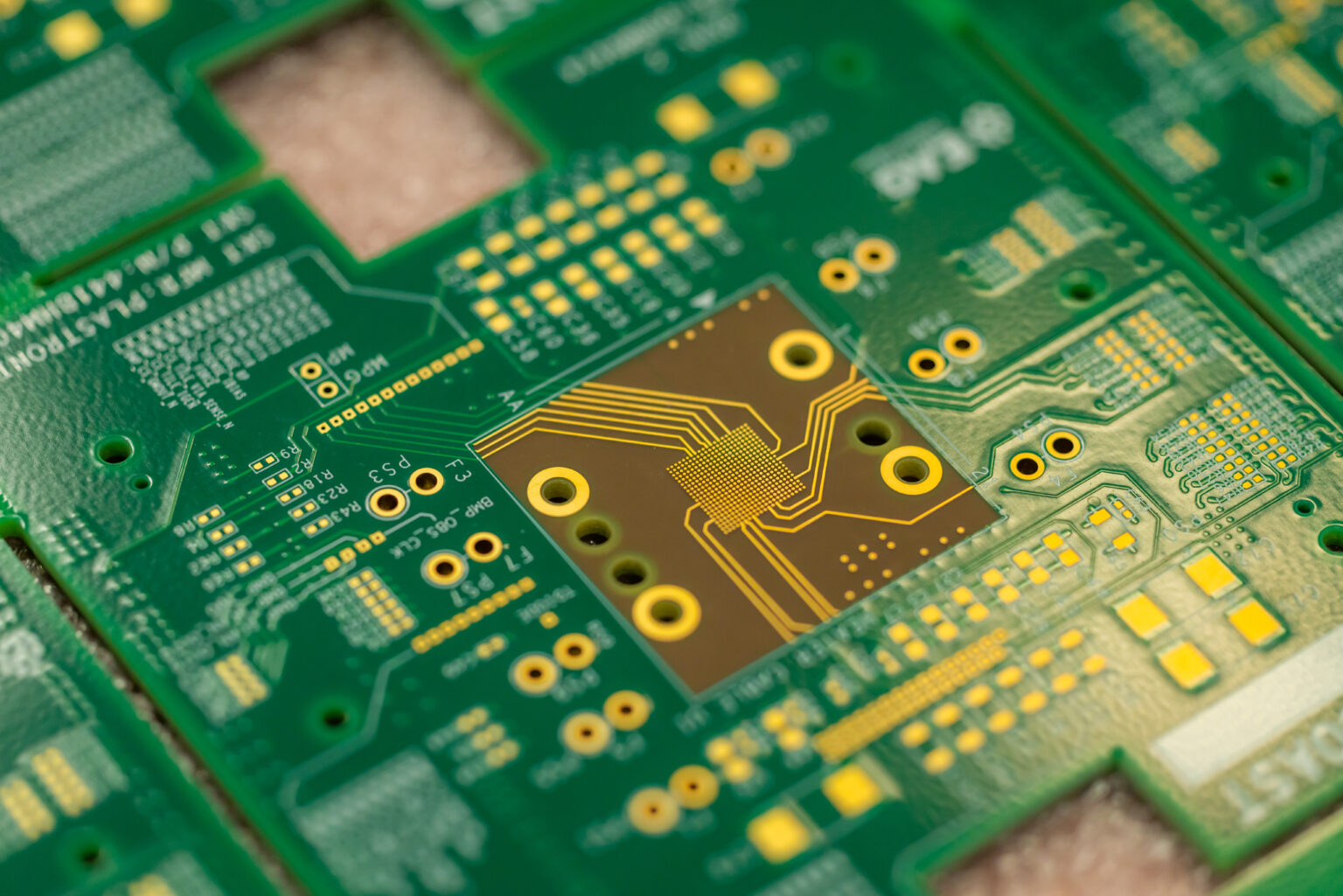
In electronics, through-hole assembly is the process of mounting leaded components onto a PCB, which involves drilling through holes. Subsequently, the components are soldered onto the pads on the opposite side of the circuit board, either manually or using an automated soldering machine.
The proportion of solder flux is carefully determined as it plays a crucial role in maintaining the quality of solder joints between the pads and component leads. During the through-hole assembly process, component leads are inserted through drilled holes from the top of the board to the bottom and then soldered.
Every through-hole assembly follows a tightly controlled manufacturing workflow with full process traceability and IPC-compliant documentation.
IPC-A-610 Class 2 & Class 3 Compliant Assembly:with certified workmanship and documented quality procedures.
Advanced Soldering Technologies:including automated wave soldering, selective soldering, robotic soldering, and precision manual soldering.
Comprehensive Inspection & Test Coverage:featuring AOI, X-ray, ICT, Flying Probe, Functional Testing, ESS, and complete production traceability.
Supports High-Reliability & Mixed Technology Assemblies:including multilayer, HDI, rigid-flex, RF, power electronics, and SMT + Through-Hole hybrid PCB assemblies.
At Altest Corporation, we provide advanced Through-Hole Technology (THT) Assembly services for electronic products requiring superior mechanical strength, high-current capability, and long-term reliability. Our manufacturing process supports complex PCB assemblies where mechanical durability and electrical robustness are critical. Utilizing automated component insertion, precision hand assembly, selective soldering, wave soldering, and IPC-certified workmanship, we manufacture through-hole assemblies that meet the stringent requirements of IPC-A-610 Class 2 and Class 3 standards for mission-critical applications.

Altest Corporation combines decades of expertise in PCB fabrication, SMT assembly, Through-Hole Assembly, Box Build Integration, and Electronics Manufacturing Services (EMS) to deliver production-ready electronic assemblies for highly regulated industries. Our manufacturing facility operates under strict quality management systems with complete material traceability, RoHS compliance, and IPC-certified assembly processes
Find answers to common questions about wave soldering, selective soldering, IPC hole-fill requirements, and mixed-technology PCBA manufacturing.
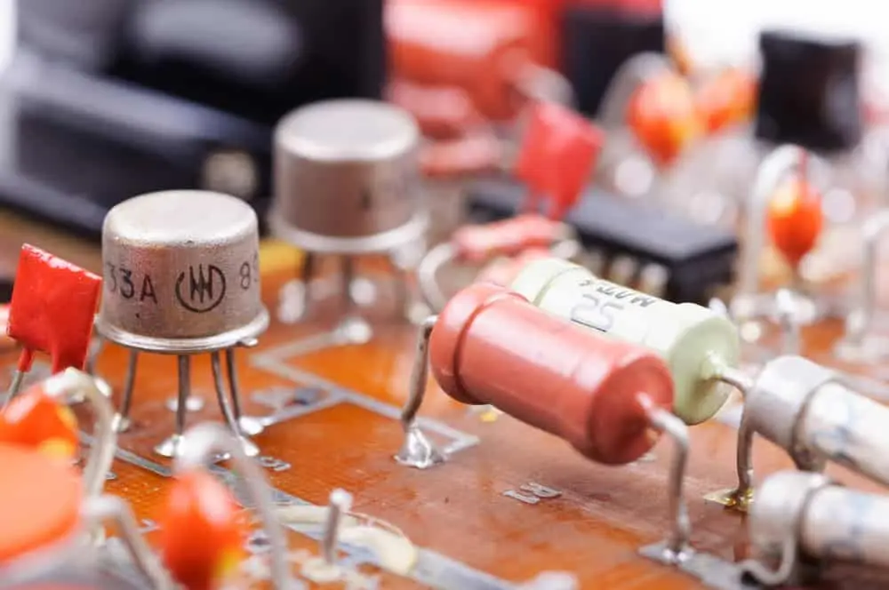
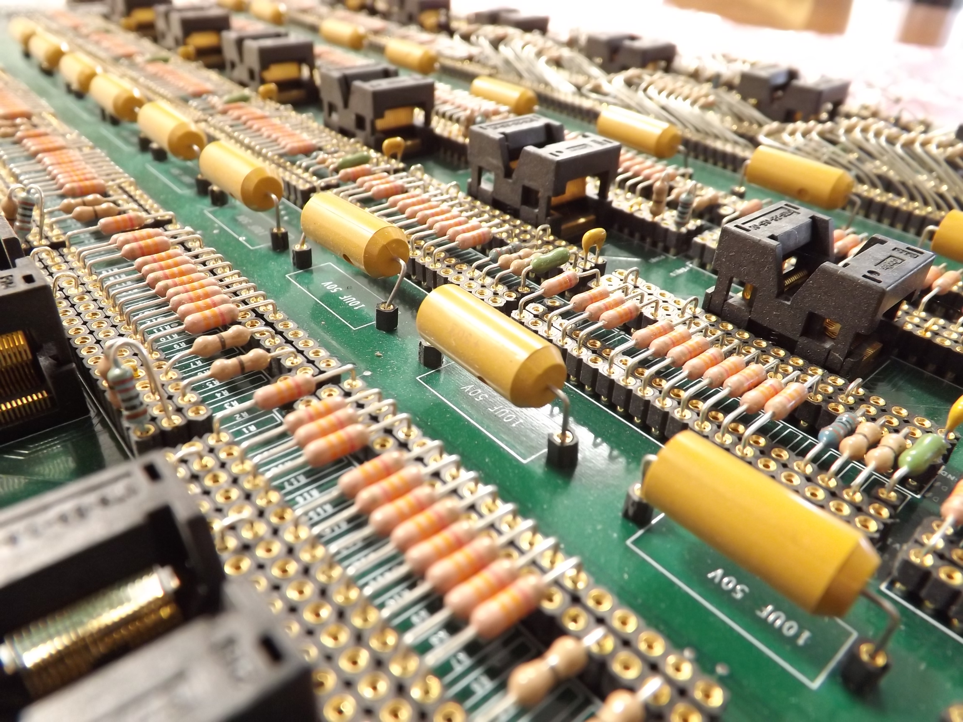
Through-Hole Technology (THT) is the process of mounting electronic components by inserting their wire leads into plated drilled holes (PTH) on a printed circuit board. The leads are then soldered to pads on the opposite side, creating an extremely strong physical and electrical bond.
While SMT dominates modern electronics, THT is absolutely critical for components that endure high physical stress (like heavy mechanical switches, large relays, and external cable connectors) or components that must handle extremely high power and voltage levels that would destroy delicate SMT pads.
We employ three primary methods depending on the board's complexity: Wave Soldering for high-volume, purely THT boards; Robotic Selective Soldering for mixed-technology boards where SMT components are nearby; and highly skilled, IPC-certified Hand Soldering for specialized or temperature-sensitive parts.
Wave soldering involves passing the bottom of a populated circuit board over a cascading "wave" of molten solder. The liquid solder wicks up into the plated through-holes via capillary action, instantly soldering hundreds of component leads in a matter of seconds. It is highly efficient for mass production.
Selective soldering uses a programmable, robotic mini-fountain of molten solder to target individual through-hole pins from the bottom of the board. It is necessary for "mixed-technology" boards, allowing us to solder THT pins without accidentally melting or damaging the tiny SMT components already placed millimeters away.
Yes. To prevent any cross-contamination, we maintain completely separate, dedicated wave soldering machines, selective solder pots, and hand-soldering stations for RoHS-compliant lead-free (SAC305) production and traditional leaded (SnPb) military/aerospace production.
This is very common. We always perform the SMT assembly (printing, pick-and-place, and convection reflow) first. Once the surface mount components are securely attached, the board moves to the through-hole department where the heavier leaded components are inserted and soldered using selective or masked wave soldering.
Our IPC-A-610 certified inspectors visually examine the top and bottom of the THT joints using high-magnification microscopes to verify proper solder wetting and fillet shape. For thick, multi-layer boards where internal barrel fill cannot be seen, we utilize 3D X-Ray (AXI) inspection.
Hole fill (or vertical capillary action) requirements depend on the standard. For standard commercial electronics (IPC Class II), we ensure at least a 50% vertical fill of solder within the plated barrel. For mission-critical aerospace, military, and medical devices (IPC Class III), we guarantee a minimum of 75% vertical fill.
Yes. We utilize automated lead forming, cutting, and bending machines. This ensures that every axial or radial component is prepared uniformly, guaranteeing consistent standoff heights from the board surface and preventing mechanical stress on the component body during insertion.
Partner with Altest Corporation for your next high-reliability PCB fabrication and turnkey SMT assembly project. Our engineering team is ready to review your gerber files and provide a detailed, competitive estimate.

