.jpg)
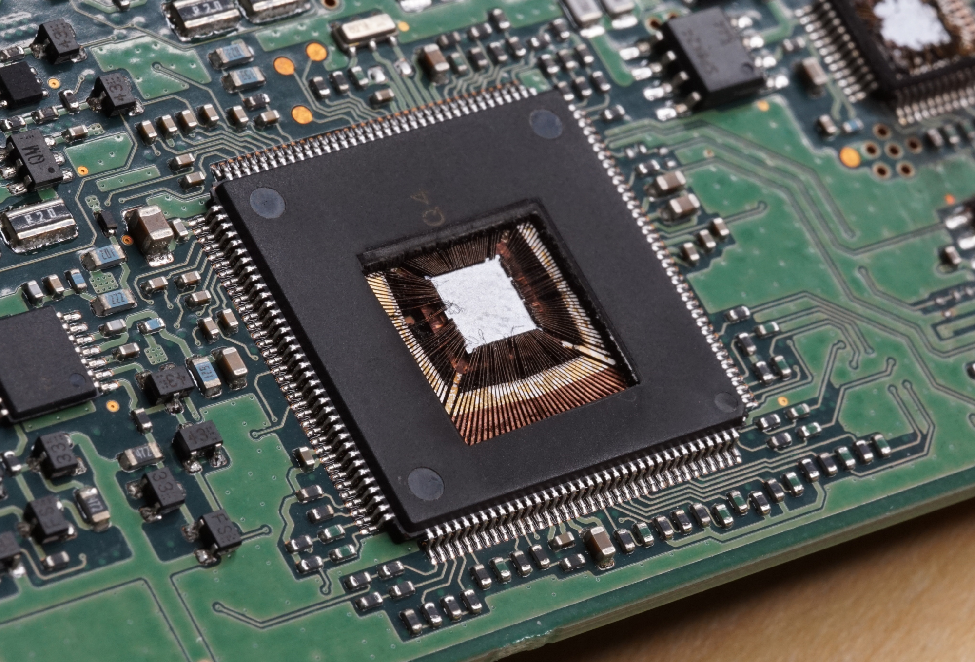
Decapsulation Testing is a crucial method in failure analysis and counterfeit detection used to examine the internal structure of integrated circuits (ICs) or other semiconductor devices. The process involves removing the protective encapsulation or plastic package from an IC or chip to expose its internal components (such as the die, bond wires, and other elements) for visual inspection and further analysis. This testing method is particularly useful for counterfeit detection, quality control, and failure investigation when there are suspicions about the authenticity or performance of electronic components.
Decapsulation provides direct access to the internal structure of an integrated circuit, enabling engineers to verify authenticity, identify hidden defects, and investigate failure mechanisms that cannot be detected through external inspection alone.
 (1).png)
Decapsulation testing involves the physical removal of the encapsulation (typically a plastic or ceramic package) of a semiconductor device to expose the internal structures, such as the die, bond wires, and solder balls. This allows engineers to inspect the component's internal design and construction, helping to verify its authenticity, identify defects, and perform failure analysis.The encapsulation is typically made of epoxy or plastic, but it can also be ceramic. The decapsulation process can involve various methods, such as chemical etching, laser ablation, or mechanical removal. Once the device is decapsulated, it can be analyzed under a microscope or with other analytical tools.
Decapsulation is one of the most effective methods for verifying the authenticity of high-value semiconductor devices. By exposing the internal die, our engineers compare die markings, manufacturer logos, fabrication identifiers, mask revisions, and internal construction against verified manufacturer data. This process enables the identification of remarked, cloned, recycled, refurbished, or substituted components that may appear authentic during external inspection but contain unauthorized or inferior semiconductor dies.
.jpg)
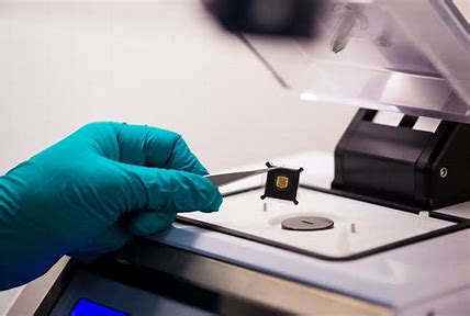
With decades of experience in electronics manufacturing, PCB testing, semiconductor analysis, and quality engineering, Altest Corporation provides precision decapsulation services using industry-recognized analytical methods and advanced laboratory equipment. Our engineering team delivers accurate, traceable reports that support failure investigations, root cause analysis, counterfeit detection, reliability testing, qualification programs, and regulatory compliance. Whether validating components for aerospace, medical devices, defense electronics, or industrial systems, we provide the engineering insight needed to ensure product integrity and long-term reliability.
Find answers to common questions about chemical etching, destructive counterfeit screening, die inspection, and AS6081 compliance.
Decapsulation is a destructive testing method used to expose the internal bare silicon die of a packaged integrated circuit. By removing the external plastic or epoxy casing, engineers can visually inspect the microscopic surface of the die to verify the true authenticity and origin of the component.
Counterfeiters often "blacktop" or remark the outside of a cheap, salvaged, or entirely different chip to look like an expensive, high-demand part. Decapsulation allows us to bypass the fake exterior and examine the manufacturer's original microscopic logo, part numbers, and copyright dates etched directly into the silicon die itself, which cannot be faked.
We typically use automated chemical decapsulation systems. This involves utilizing highly controlled, heated corrosive acids—such as fuming nitric acid or fuming sulfuric acid—to selectively melt and etch away the plastic mold compound (epoxy resin) without damaging the delicate silicon die or the connecting wire bonds.
Yes, decapsulation is strictly a destructive test. The specific component subjected to the acid etching has its physical package compromised and cannot be placed on a production PCB. This is why we perform decapsulation on a statistically significant random sample from a larger batch of components, rather than the entire reel.
No. Our automated decapsulation equipment precisely controls the acid temperature, volume, and etch time. Fuming nitric and sulfuric acids rapidly dissolve the carbon-based epoxy packaging but do not react with the silicon die or gold wire bonds, leaving them in pristine condition for high-magnification optical inspection.
Using high-power metallurgical microscopes, we compare the exposed die against a known authentic "golden" component or the original manufacturer's die database. We verify the specific die size, the topography of the metallization patterns, the layout of the wire bond pads, and the microscopic manufacturer markings.
Ceramic and metal-can packages cannot be chemically decapsulated using acids because they do not use epoxy resin. Instead, they undergo a mechanical process called "de-lidding." We use specialized mechanical milling, grinding, or thermal prying techniques to physically remove the metal or ceramic lid and expose the die inside.
Partial decapsulation etches a small, localized cavity just over the center of the die to expose the manufacturer markings while leaving the rest of the package and wire bonds intact. Full decapsulation strips away almost all the molding compound, fully exposing the die and all wire bonds for comprehensive structural analysis and failure testing.
Surprisingly, yes. If performed correctly via partial decapsulation, the internal electrical pathways (wire bonds) remain intact. The component can often still be placed into a specialized socket for electrical curve tracer testing to further verify its operational integrity, even though it can never be used in a final product.
Decapsulation is a mandatory core requirement for high-reliability counterfeit mitigation programs. Our decapsulation protocols strictly adhere to aerospace and defense standards, including SAE AS6081, AS6171, and IDEA-STD-1010. This ensures absolute confidence in your supply chain when sourcing from independent brokers.
Partner with Altest Corporation for your next high-reliability PCB fabrication and turnkey SMT assembly project. Our engineering team is ready to review your gerber files and provide a detailed, competitive estimate.

