 (1).jpg)
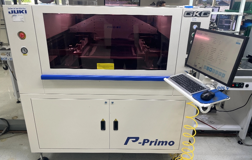

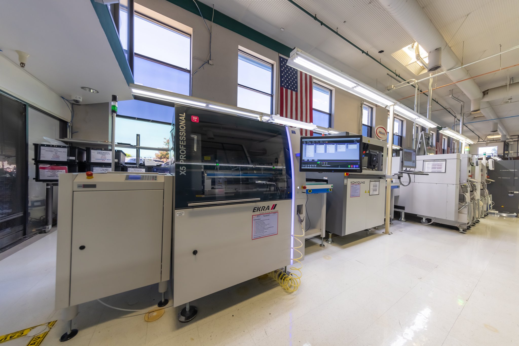
Solder Paste stencil printers help precisely place solder paste where you want it on your printed circuit board without a mess or hassle.
Solder Paste Stencil Printer EKRA and JUKI.
Ensures precise and consistent application of solder paste, improving the quality of solder joints and reducing defects.
Increases production efficiency by speeding up the paste application process, minimizes waste, and ensures uniform coverage, especially for fine-pitch components
Accurate solder paste deposition is the foundation of every successful SMT assembly. Our Solder Paste Stencil Printing process minimizes printing defects, enhances solder joint integrity, and improves manufacturing efficiency, ensuring every PCB assembly is built for maximum performance, durability, and reliability.

Our stencil printing systems are designed to handle everything from standard SMT assemblies to ultra-fine pitch and high-density PCB designs. We utilize laser-cut stainless-steel stencils, automatic fiducial alignment, programmable squeegee pressure, controlled print speed, and precision stencil separation to achieve uniform solder paste deposition across every PCB. Our capabilities support 01005 passive components, QFN, BGA, CSP, Micro BGA, LGA, fine-pitch ICs, and high-density interconnect (HDI) assemblies, ensuring exceptional print quality even on the most complex circuit boards.
To maintain consistent print quality, every stencil printing operation is monitored using strict process controls and IPC-compliant manufacturing practices. Our quality procedures include Solder Paste Inspection (SPI), stencil cleanliness verification, paste height measurement, volume analysis, offset inspection, bridging detection, and print repeatability monitoring. These inspections help identify defects before component placement, significantly reducing rework while improving first-pass yield and long-term assembly reliability.
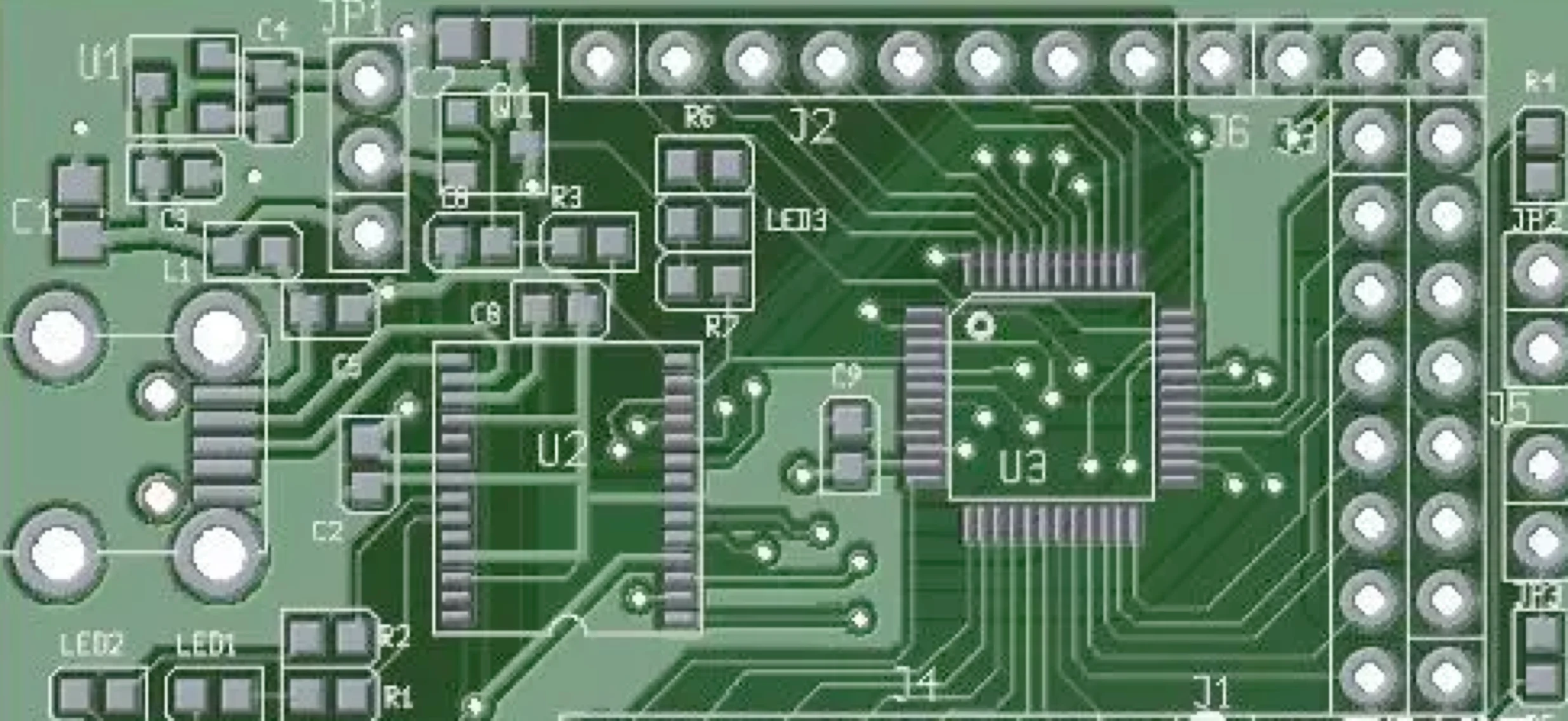
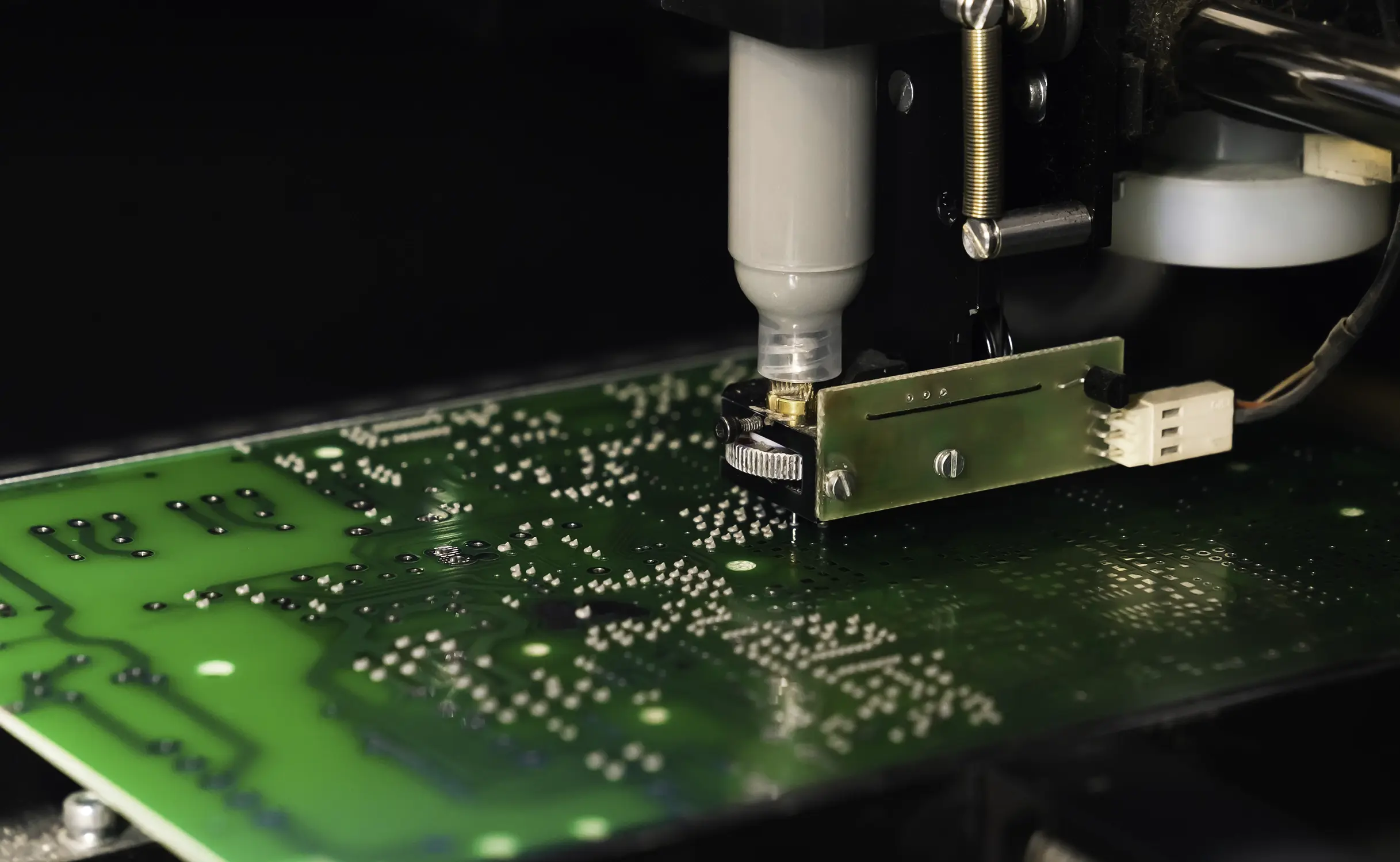
With decades of experience in PCB assembly and electronics manufacturing, Altest Corporation combines advanced SMT equipment, experienced process engineers, and rigorous quality control to deliver exceptional solder paste printing performance. Whether manufacturing prototypes, low-volume production, or high-volume commercial assemblies, our automated printing process ensures superior consistency, optimized solder joint formation, and reliable electronic products that meet the highest IPC quality standards.
Find answers to common questions about laser-cut stencils, nano-coatings, aperture design, and 3D Solder Paste Inspection (SPI).
Solder paste stencil printing is the first and most critical step in the Surface Mount Technology (SMT) assembly process. It involves using a precision squeegee blade to push specialized solder paste through the apertures (holes) of a metal stencil, depositing exact volumes of paste directly onto the PCB's copper pads before component placement.
Industry studies show that over 70% of all SMT defects (such as solder shorts, bridging, tombstoning, or open connections) originate from a poor solder paste printing process. Controlling the exact volume, height, and alignment of the paste deposit is fundamental to achieving high-yield, zero-defect manufacturing.
Our standard stencils are manufactured from high-tension stainless steel. For high-precision requirements, we utilize laser-cut stencils with electropolished walls to ensure smooth paste release. For extreme fine-pitch applications, we use electroformed nickel stencils, which offer the highest degree of aperture smoothness and precision.
A step stencil features varying thicknesses across the same metal sheet. It is used when a single PCB requires large volumes of solder paste for heavy components (like power connectors) but simultaneously needs very small, precise volumes of paste for ultra-fine pitch components (like micro-BGAs). The stencil is "stepped up" or "stepped down" in specific regions to accommodate both.
We use fully automated, inline screen printers equipped with high-resolution CCD cameras. These cameras locate global and local fiducial markers on both the PCB and the stencil. The machine's robotic vision system then calculates and adjusts the X, Y, and Theta (rotation) offsets to achieve sub-micron alignment accuracy before lowering the stencil.
SPI is a crucial quality assurance step performed immediately after the printing process. Using a 3D Automated Solder Paste Inspection machine, we scan 100% of the printed pads to measure the exact volume, height, area, and positional offset of the deposited paste. Any board failing these strict mathematical tolerances is instantly rejected.
We use premium Type 4 and Type 5 solder pastes, which feature smaller, more uniform powder particle sizes required for densely packed HDI boards. We stock both RoHS-compliant lead-free pastes (like SAC305) and traditional leaded pastes (SnPb) for aerospace and military applications requiring tin-whisker mitigation.
Nano-coating is a specialized, flux-repellent chemical layer applied to the bottom and aperture walls of the stencil. It prevents paste from sticking to the stencil, drastically improving transfer efficiency (paste release) for ultra-small apertures like 01005 discretes or 0.3mm pitch BGAs, while also reducing the frequency of under-stencil wiping.
Solder paste rheology (viscosity and tackiness) is highly sensitive to environmental changes. Our printing facilities are strictly climate-controlled, maintaining optimal temperature (20-25°C) and relative humidity (40-60%) to prevent the paste flux from drying out or absorbing ambient moisture.
Because SPI happens *before* component placement and reflow, a failed board is easily recovered. We simply pull the board from the line, clean off the wet solder paste using specialized solvents, dry it completely, and run it through the printer again. This closed-loop process prevents costly rework down the line.
Partner with Altest Corporation for your next high-reliability PCB fabrication and turnkey SMT assembly project. Our engineering team is ready to review your gerber files and provide a detailed, competitive estimate.

