.jpg)
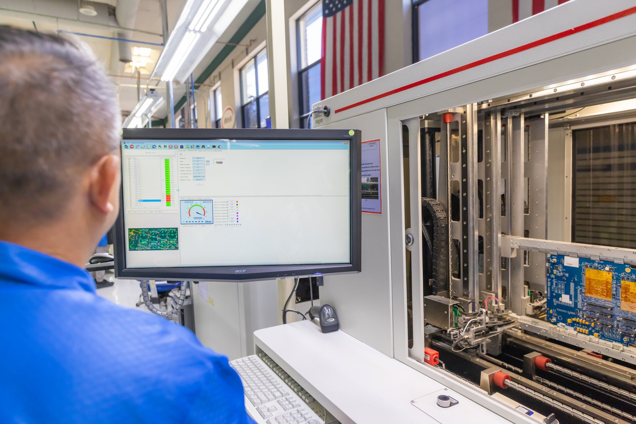
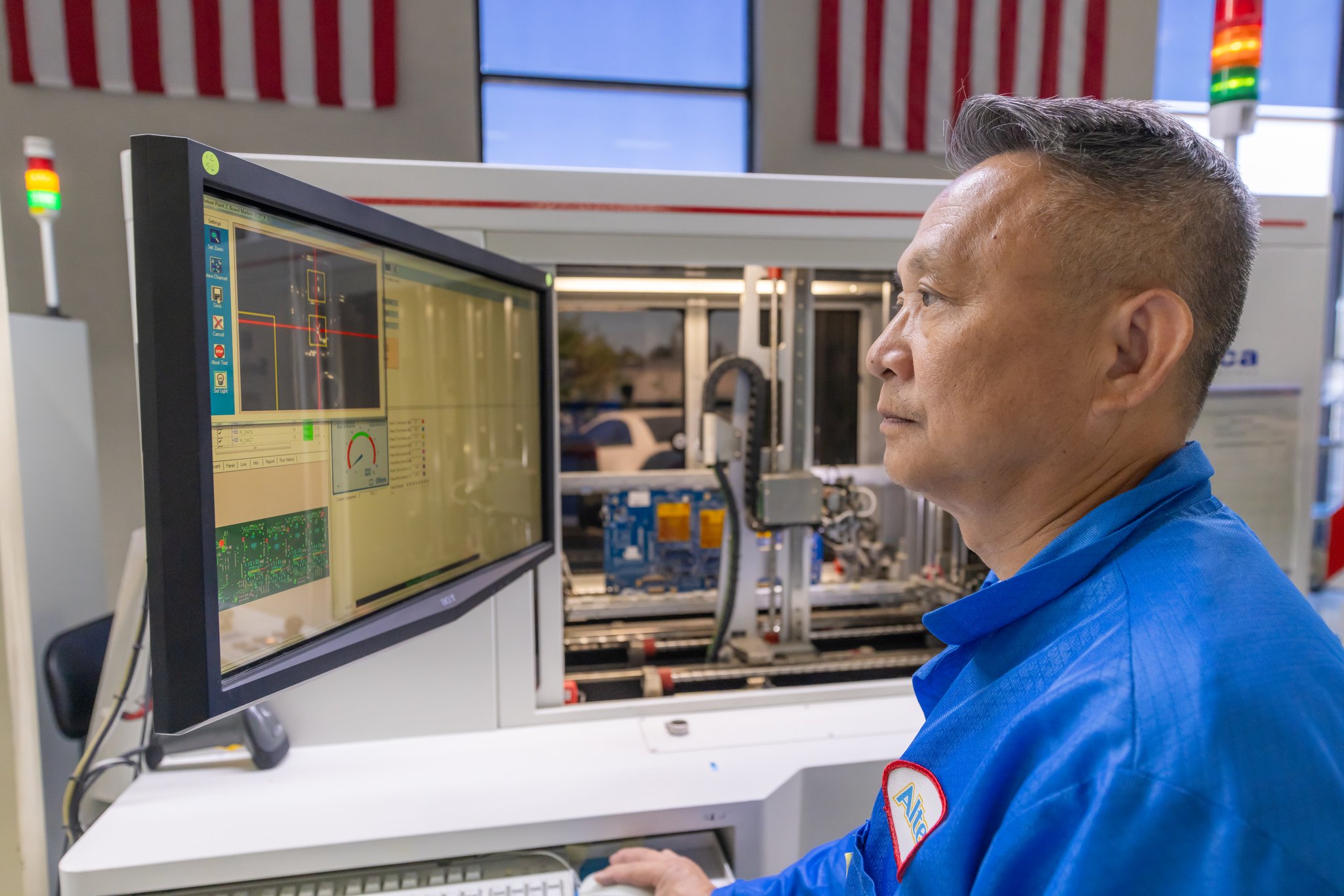
Our Flying Probe systems employ multiple independently controlled probes capable of accessing test points on both sides of the PCB with micron-level positioning accuracy. The system performs a wide range of electrical measurements, including continuity testing, open circuit detection, short circuit detection, resistance measurement, capacitance testing, diode verification, transistor analysis, inductance measurement, polarity verification, isolation testing, and powered functional checks. By comparing measured values against CAD netlists and test programs, we ensure every electrical connection conforms to the original design specifications.
CAD data: ODB++, IPC, Allegro BRD (ASCII), … Detect Open / Short on PCBAs Verify values of Resistors, Capacitors,Inductors Functional Test: Relays, LED, Diodes, DC Power Controlled ICs Number of Electrical Probes: 4 front, 4 rear Maximum Board Size: 21.25 × 24”

Fixtureless Electrical Testing:Eliminates the cost and lead time associated with custom ICT fixtures, making it ideal for prototypes and low-volume production.
High Test Coverage:Detects opens, shorts, incorrect component values, polarity errors, missing components, and solder-related electrical faults with high accuracy
CAD-Driven Test Programming:Generates automated test routines directly from PCB design data, reducing engineering time and accelerating product validation.
Supports Complex PCB Technologies:Qualified for multilayer, HDI, rigid-flex, RF/microwave, high-speed digital, and mixed SMT/Through-Hole PCB assemblies.
Flying Probe Testing provides extensive electrical coverage throughout the manufacturing process, particularly for high-density, multilayer, HDI, rigid-flex, RF, and complex mixed-technology PCB assemblies where traditional bed-of-nails fixtures may not be practical. Our testing process is integrated with Automated Optical Inspection (AOI), Solder Paste Inspection (SPI), X-Ray Inspection (AXI), In-Circuit Testing (ICT), Functional Testing (FCT), and Statistical Process Control (SPC) to deliver complete manufacturing verification. Every PCB assembly is tested using customized test programs to detect opens, shorts, incorrect component values, solder defects, and assembly-related electrical failures before final product integration.

With decades of expertise in PCB manufacturing, assembly, and electronic testing, Altest Corporation provides advanced Flying Probe Testing solutions that ensure exceptional product quality and reliability. Our engineering team develops optimized test programs directly from CAD and Gerber data, enabling rapid setup, reduced testing costs, and faster product qualification. Whether supporting engineering prototypes, aerospace electronics, medical devices, industrial controls, telecommunications infrastructure, automotive electronics, or defense systems, we deliver highly accurate electrical testing that minimizes manufacturing risk and maximizes first-pass yield.
Find answers to common questions about fixtureless testing, soft-touch technology, bare board vs. PCBA testing, and the advantages of flying probe over traditional ICT.
Flying Probe Testing is an automated, electro-mechanical testing method used to verify the electrical integrity of both bare PCBs and populated PCBAs. It uses robotic "flying" probes—highly precise, movable test needles—to make contact with test points, vias, and component pads on the board to measure resistance, capacitance, inductance, and identify shorts or opens.
Traditional ICT (Bed-of-Nails) requires a custom, expensive physical fixture with hundreds of stationary pins built specifically for one board design. Flying Probe is fixtureless, using software-controlled moving probes. This makes FPT ideal for prototypes, low-to-medium volume runs, and high-density boards where a physical fixture would be too costly or take too long to build.
For bare boards, it detects electrical opens and shorts between traces. For assembled boards (PCBAs), it can verify component values (resistors, capacitors, diodes), check for missing or incorrect components, verify diode/transistor polarity, and detect manufacturing defects like solder bridges or dry joints.
While having dedicated test pads makes testing easier, one of the main advantages of FPT is its sub-micron precision. Modern flying probes can accurately contact component leads, vias, and microscopic solder joints without needing dedicated test pads, which is crucial for densely packed, miniaturized High-Density Interconnect (HDI) boards.
Yes. Advanced flying probe machines use "soft-touch" technology. The probes are equipped with sophisticated Z-axis sensors that control the exact amount of mechanical pressure applied to the board. This prevents physical damage or piercing to delicate SMT pads, fine-pitch BGA substrates, and sensitive component leads.
High-end, modern Flying Probe testers feature dual-sided testing capabilities. They have multiple moving probes positioned on both the top and bottom of the board, allowing for comprehensive 360-degree electrical testing and component verification in a single pass without needing an operator to manually flip the PCBA.
While traditionally used for unpowered (cold) in-circuit testing, advanced flying probe systems can apply power to specific nets. This allows our engineers to perform limited boundary scan (JTAG) testing, embedded memory programming, and basic functional tests on specific ICs, oscillators, and voltage regulators right on the tester.
Because the probes must physically move to each test point sequentially, FPT is slower than a fixture-based ICT (which tests all points instantly and simultaneously). Depending on the board's complexity, net count, and the number of components, an FPT cycle can take anywhere from a few minutes to over 15 minutes per board.
It is used in two key phases. First, in bare board fabrication: every manufactured PCB undergoes bare-board FPT before any components are placed to guarantee no hidden trace shorts or opens. Second, in assembly (PCBA): the fully populated board is tested after SMT reflow and inspection to verify every solder joint and component is electrically sound.
To program the FPT machine with extreme accuracy, we require your intelligent CAD data (such as ODB++ or IPC-2581 files), or a combination of standard Gerber RS-274X files, the IPC-D-356 netlist, the full Bill of Materials (BOM), and the XY coordinate (centroid) data for component placement.
Partner with Altest Corporation for your next high-reliability PCB fabrication and turnkey SMT assembly project. Our engineering team is ready to review your gerber files and provide a detailed, competitive estimate.

