
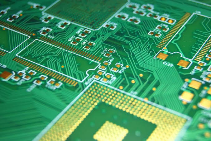
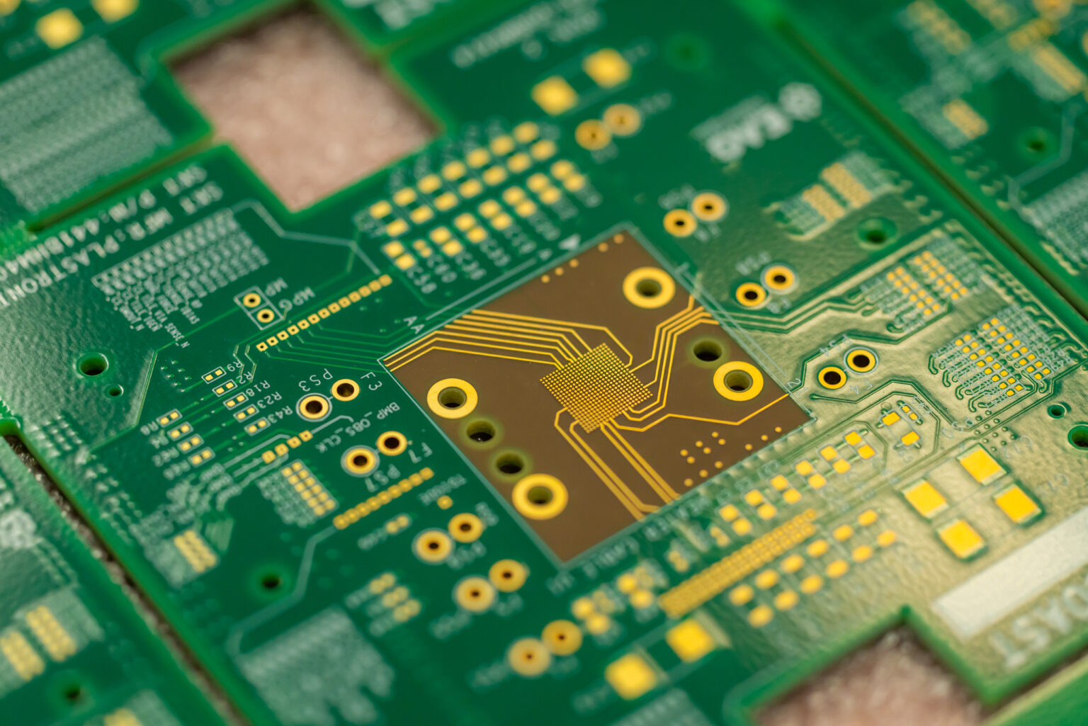
Our burn-in laboratory is equipped with programmable environmental chambers, automated monitoring systems, and custom burn-in fixtures capable of supporting a wide range of electronic products. Throughout the burn-in cycle, critical operating parameters—including temperature, voltage, current consumption, clock frequency, communication interfaces, and system functionality—are continuously monitored and recorded.
PCB layout engineering requires careful consideration of several factors to ensure the final board meets performance, manufacturability, and reliability standards.
.jpg)
Static Burn-In Testing
Dynamic Burn-In Testing
High-Temperature Operating Life (HTOL)
Power Cycling
Thermal Soak Testing
Functional Burn-In
Functional Burn-In
Following burn-in, every assembly undergoes comprehensive verification to confirm operational integrity and long-term reliability. Our quality assurance workflow integrates Functional Testing (FCT), Automated Optical Inspection (AOI), X-Ray Inspection (AXI), In-Circuit Testing (ICT), Flying Probe Testing, and Electrical Verification to ensure that no degradation or failures have occurred during stress testing.
Our engineering team has extensive experience developing customized burn-in procedures for highly regulated industries requiring maximum product reliability. We design application-specific burn-in profiles based on JEDEC, MIL-STD, IPC, and customer-defined reliability requirements, ensuring every product receives the appropriate level of stress screening without exceeding component limitations.
Find answers to common questions about infant mortality screening, dynamic vs. static burn-in, high-temperature substrates, and custom burn-in board fabrication.
Burn-In Testing is an extreme stress-testing process where populated circuit boards or individual semiconductors are subjected to elevated temperatures and operating voltages inside a specialized oven. The goal is to artificially accelerate the lifecycle of the components to weed out early failures before the product is shipped to the end-user.
In reliability engineering (the "Bathtub Curve"), infant mortality refers to products that fail very early in their operational life due to latent manufacturing defects—such as weak wire bonds, dielectric flaws, or metallization issues. Burn-in testing forces these weak components to fail safely in the factory rather than catastrophically in the field.
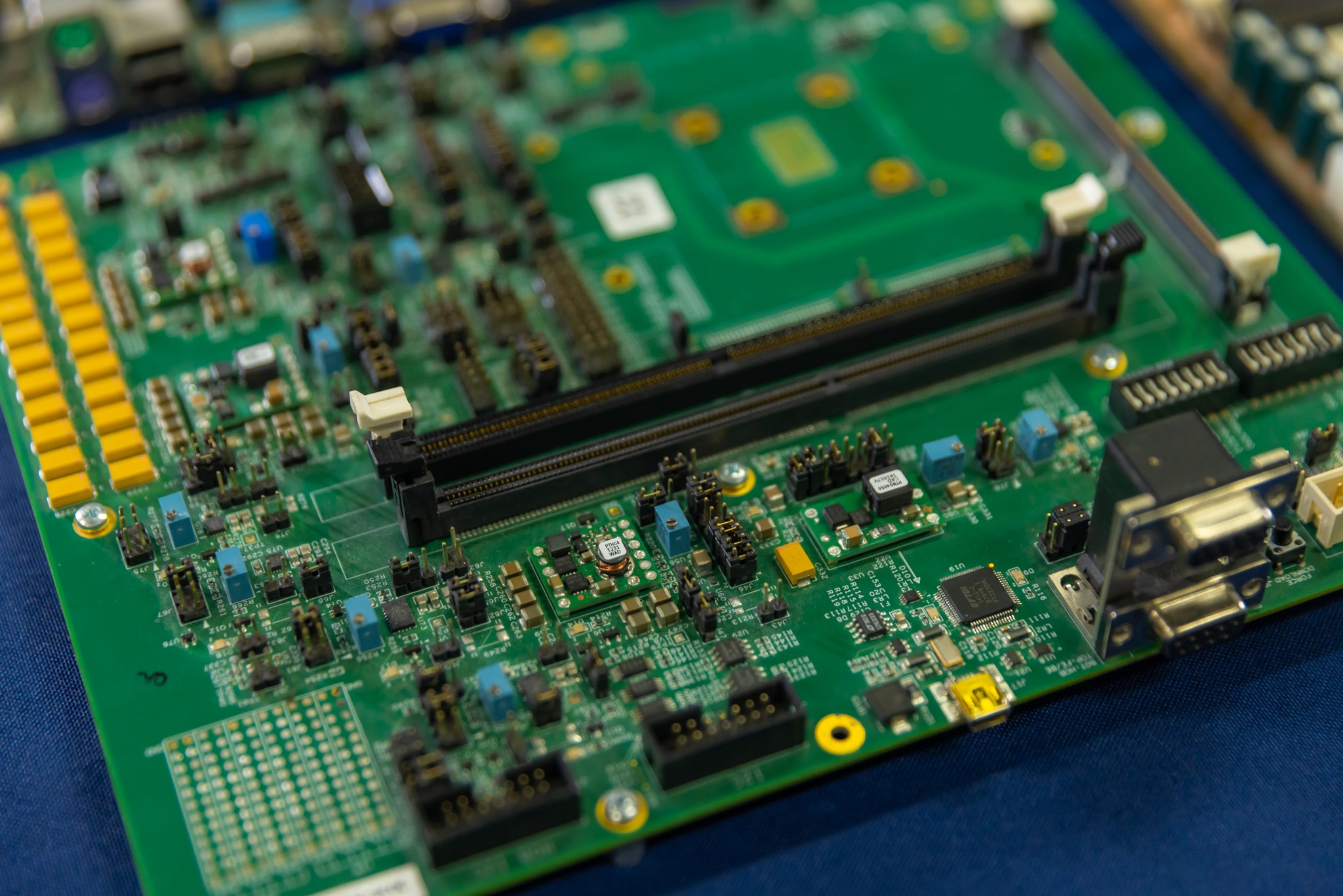
A Burn-In Board (BIB) is a highly specialized, heavy-duty printed circuit board designed to hold multiple Device Under Test (DUT) components or smaller PCBAs inside the burn-in oven. It acts as the electrical interface, routing the high voltages and test signals from the oven's external stimulus generators directly to the components being stressed.
Static burn-in simply applies extreme heat and a constant extreme voltage to the components; it tests thermal and dielectric limits but does not exercise the logic. Dynamic burn-in applies heat and voltage, but also inputs active electronic signals (clock cycles, data) to fully exercise the component's internal logic gates while under extreme thermal stress.
Because these boards must survive hundreds of hours at 125°C to 150°C (or higher), standard FR-4 is not suitable as it will warp and degrade. We manufacture Burn-In Boards using ultra-high Tg (Glass Transition Temperature) polyimide, High-Tg FR-4, or specialized BT epoxy resins that can withstand thousands of hours of continuous extreme heat without failing.
Yes. We provide end-to-end burn-in solutions. Our engineering team designs the BIB layout to fit your specific oven dimensions and slot requirements, selects the appropriate high-temperature test sockets for your package type, fabricates the heavy-copper board, and assembles it completely in-house.
The duration depends entirely on the reliability standard being followed and the end-use application. Commercial screening might require 24 to 48 hours at 125°C. For mission-critical military or aerospace components, burn-in cycles can extend to 168 hours (1 week) or more of continuous thermal and electrical stressing.
It is highly mandated in industries where failure is not an option. This includes Aerospace (satellites, avionics), Defense/Military (radar, weapons systems), Medical Devices (life-support systems, implants), Automotive (EV powertrain controllers), and high-reliability data centers.
Yes. Testing modern, high-power components means the devices themselves generate massive amounts of heat inside the oven. We design our Burn-In Boards with heavy copper traces, thermal vias, and specialized heat sinks to manage thermal runaway and ensure precise, uniform temperature control across every DUT on the board.
Our burn-in procedures are typically governed by MIL-STD-883 (Test Method Standard, Microcircuits) and JEDEC standard JESD22-A108. We also develop customized burn-in and environmental stress screening (ESS) protocols tailored directly to your specific OEM or industry compliance requirements.
Partner with Altest Corporation for your next high-reliability PCB fabrication and turnkey SMT assembly project. Our engineering team is ready to review your gerber files and provide a detailed, competitive estimate.

