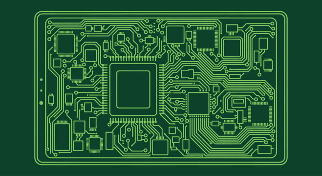
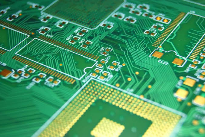
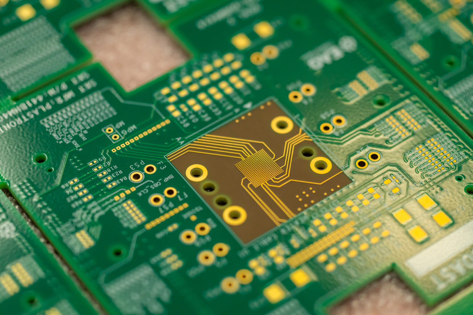
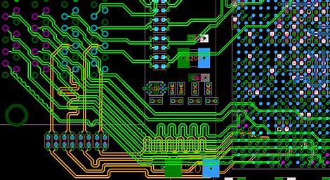
Transform your electronic concepts into production-ready PCB designs with our Schematic Capture Services. At Altest Corporation, our experienced engineers develop clear, accurate, and fully documented electronic schematics that serve as the foundation for reliable PCB layout, manufacturing, testing, and assembly. From simple analog circuits to complex high-speed digital systems, we create intelligent schematics that reduce design errors, accelerate product development, and ensure seamless collaboration throughout the engineering process.
Our schematic capture process follows industry best practices and IPC standards, helping businesses shorten development cycles while improving product performance, manufacturability, and long-term reliability.
Our structured engineering workflow ensures every schematic is complete, verified, and ready for PCB layout and manufacturing.
Analysis: We review product specifications, functional requirements, electrical architecture, and design objectives before beginning schematic development.
Circuit Design & Component Selection:Our engineers create logical circuit diagrams while selecting reliable, cost-effective, and readily available electronic components.
Library & Symbol Creation:Custom schematic symbols and PCB footprints are developed when standard libraries are unavailable, ensuring consistency and manufacturing accuracy.
Electrical Rule Check (ERC):Every schematic undergoes comprehensive validation to identify missing connections, incorrect pin assignments, power conflicts, and logical errors before PCB layout begins.
Documentation & BOM Generation:We deliver organized schematic files, hierarchical documentation, netlists, manufacturing-ready design files, and a complete Bill of Materials (BOM) for procurement and production.
With decades of PCB engineering experience, Altest Corporation delivers high-quality schematic capture solutions for projects ranging from prototype development to high-volume production. Our multidisciplinary team works closely with clients to create scalable, manufacturable, and testable electronic designs that meet the highest standards of quality and performance.
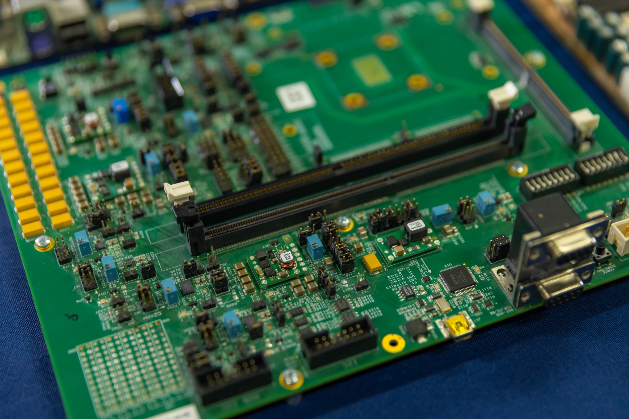
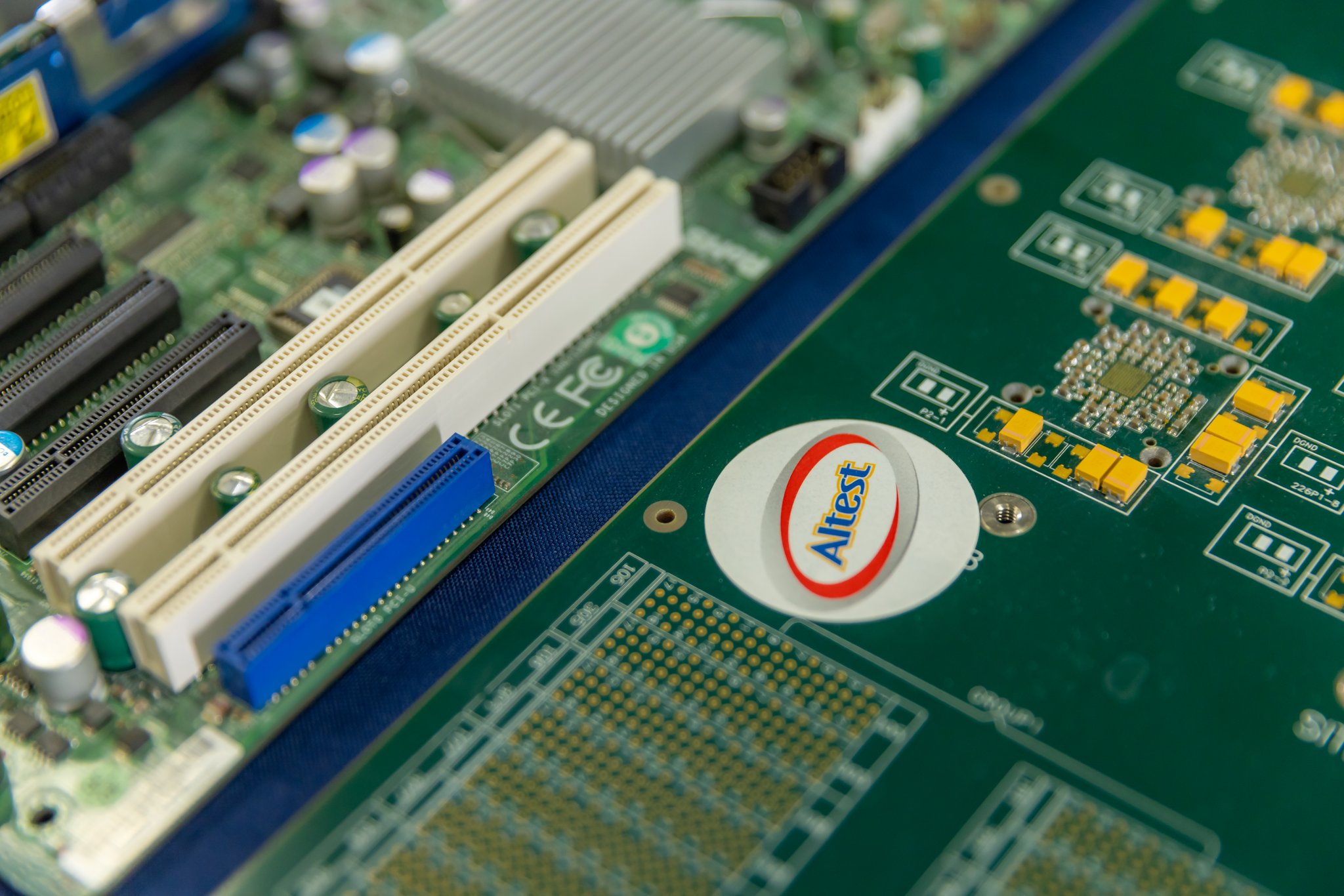
We support a wide range of technologies, including multilayer PCBs, HDI boards, RF and microwave circuits, high-speed digital systems, embedded electronics, power electronics, medical devices, aerospace applications, and industrial control systems. By integrating schematic capture with PCB layout, DFM, DFT, PCB fabrication, and PCB assembly services, we provide a complete end-to-end electronic product development solution that reduces risk, shortens time-to-market, and ensures superior product reliability.
Find answers to common questions about our schematic design, legacy conversions, and netlist validation services.
Schematic capture is the first critical step in the PCB design process. It involves translating your logical electronic circuit designs, hand-drawn sketches, or block diagrams into a strict, digital computer-aided design (CAD) format. This creates the exact electrical netlist used to route the physical board.
We maintain native support for industry-leading CAD environments to ensure seamless handoffs. Our primary tools include Altium Designer, Cadence Allegro, and Mentor Graphics PADS. We can export to almost any standard format your team requires.
We are highly flexible. You can provide us with anything from napkin sketches and PDF block diagrams to legacy CAD files or partially completed design notes. We also require a preliminary Bill of Materials (BOM) and your specific component datasheets.
Yes. During the schematic capture phase, we link all logical symbols directly to manufacturer part numbers (MPNs). We perform obsolescence checks and lifecycle tracking to ensure the components in your design are actively procurable for manufacturing.
If our database flags a component as EOL (End of Life) or out-of-stock, our engineering team immediately sources suitable drop-in replacements. We will always seek your authorization before altering the schematic to accommodate a substitute part.
Absolutely. If you have outdated schematics built in obsolete software (or existing only as PDFs), we can perform a full digital translation. We will rebuild the libraries, redraw the logic paths, and export the file into a modern format like Altium Designer.
We use rigorous Design Rule Checking (DRC) and Electrical Rule Checking (ERC) built into our CAD tools. This automatically detects open circuits, floating pins, shorted nets, and logical errors before the design is ever sent to layout.
Yes. Using advanced tomographic scanning and netlist extraction techniques, our engineers can reverse-engineer a completely undocumented physical PCB back into a fully functioning digital schematic and component library.
Yes, we offer SPICE and signal integrity simulations for critical RF, analog, or high-speed digital pathways. Simulating the schematic logic allows us to verify power distribution and signal performance before proceeding to PCB layout.
You do. Upon project completion and sign-off, Altest Corporation transfers full ownership of all native source files, PDF exports, custom component libraries, and generated netlists entirely to you.
Partner with Altest Corporation for your next high-reliability PCB fabrication and turnkey SMT assembly project. Our engineering team is ready to review your gerber files and provide a detailed, competitive estimate.

