

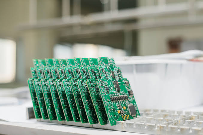
In the highly competitive world of electronics manufacturing, speed to market is often the deciding factor between securing market share and falling behind. However, speed cannot come at the expense of quality. This is where professional PCB prototype manufacturing becomes the most critical phase of the product development lifecycle.
A printed circuit board prototype is much more than just a proof of concept. It is the physical manifestation of months of engineering, simulation, and design. At Altest Corporation, our dedicated New Product Introduction (NPI) teams specialize in turning complex CAD data into fully functional, testable hardware in a matter of days. We understand that your engineering teams are relying on these initial boards to validate logic, perform thermal stress tests, and verify signal integrity before committing to expensive, high-volume production runs.
Whether you are an aerospace contractor testing a new RF communication array or a medical device startup validating a wearable biometric sensor, partnering with a responsive, USA-based PCB prototyping facility ensures that your intellectual property is protected and your design feedback loop is as short as possible.
The Importance of Rapid PCB Prototyping in Electronics Development
Attempting to bypass the prototyping phase and jump straight into mass production is an incredibly risky endeavor. In modern electronics, the margins for error are microscopic. A single incorrect footprint, a slight mismatch in differential impedance, or a localized thermal hotspot can render an entire batch of tens of thousands of boards completely useless.
A rigorous PCB prototype phase acts as your ultimate insurance policy. It allows your engineering team to physically probe the board, run electrical testing (such as flying probe and in-circuit tests), and ensure the firmware interacts correctly with the physical hardware. Furthermore, prototyping exposes potential manufacturability issues early. If a specific component is difficult to source or causes soldering defects during the SMT process, our engineers will catch it during the prototype build and suggest Design for Manufacturability (DFM) adjustments before volume scaling begins.
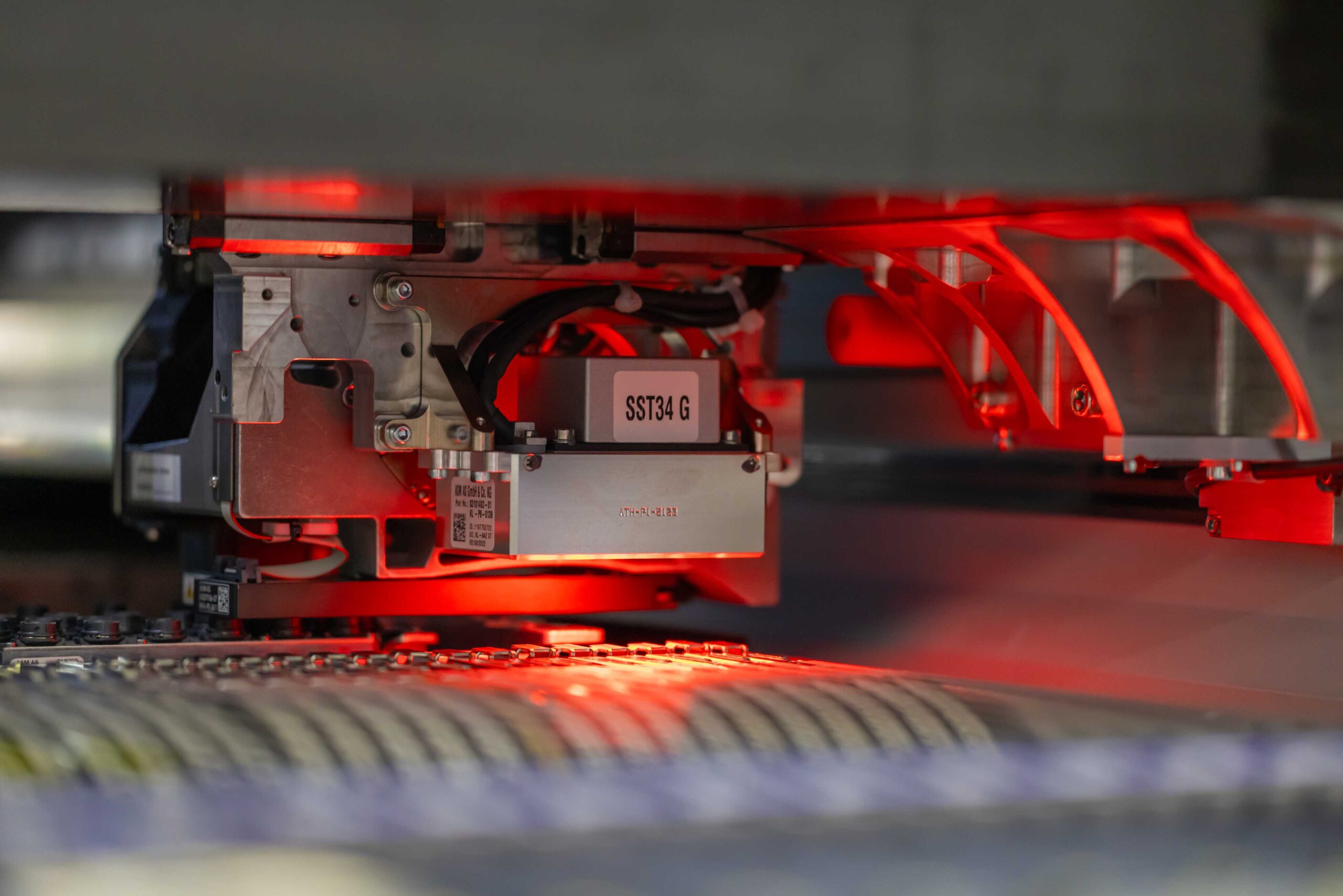
Altest Corporation’s PCB Prototyping Capabilities
Prototyping often involves pushing the boundaries of what is technologically possible. Because we operate state-of-the-art fabrication and assembly equipment, Altest Corporation can support the most demanding architectural constraints required by modern printed circuit board prototypes.
Quick-Turn Bare Board Fabrication
We offer accelerated fabrication services for bare boards. Depending on the layer count and material complexity, we can turn around raw PCBs in as little as 24 to 48 hours. We support a wide array of dielectric materials, including standard FR-4, high-frequency Rogers materials for RF applications, and specialized polyimides for flexible circuits. Every prototype board undergoes standard electrical testing (E-Test) to guarantee zero shorts or opens before it ever reaches the assembly line.
Prototype PCB Assembly (PCBA)
Having the bare board is only half the battle. Our facility features dedicated prototype Surface Mount Technology (SMT) lines specifically configured for rapid changeovers rather than steady-state volume. This allows us to populate your PCB prototype with ultra-fine pitch components, Micro-BGAs, and 01005 passive chips quickly and accurately. We also provide manual and selective wave soldering for robust through-hole components.
High-Density Interconnect (HDI) & Complex Multilayers
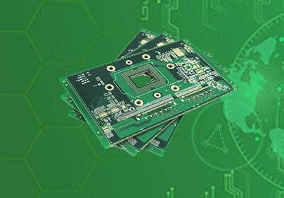
As devices shrink, prototypes are becoming increasingly complex. We routinely manufacture HDI prototypes featuring blind and buried vias, laser-drilled microvias, and sequential lamination cycles. If your design requires a 24-layer communications backbone with strict impedance control, our engineering team has the experience to build it right the first time.
Flex and Rigid-Flex Prototypes
For applications where spatial constraints require the board to fold or bend—such as in camera modules, aerospace sensors, or medical wearables—we offer comprehensive flex and rigid-flex prototyping. We help you validate the bend radius, coverlay application, and mechanical resilience of your flexible design before you finalize the mechanical enclosure.
The PCB Prototyping Process: From Concept to Physical Board
To ensure speed without sacrificing reliability, Altest Corporation utilizes a highly structured, phase-gated approach to every PCB prototype project.
- DFM and DFA Review: The moment we receive your Gerber data and Bill of Materials (BOM), our engineering team runs an extensive Design for Manufacturability (DFM) and Design for Assembly (DFA) review using advanced software like Valor NPI. We identify acid traps, solder mask slivers, and potential tombstoning risks before cutting any material.
- Component Sourcing & Procurement: Sourcing components for a small prototype run can be challenging due to minimum order quantities (MOQs) and global shortages. Our procurement team leverages our extensive supply chain network to locate the exact active and passive components you need, or we can suggest readily available drop-in replacements to keep your project on schedule.
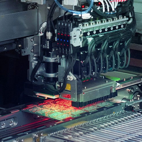
- Fabrication & Assembly: Once materials are secured, the boards are fabricated and routed to our dedicated NPI assembly cells. Here, our technicians use precise solder paste printing, automated pick-and-place machinery, and carefully profiled reflow ovens to build your boards.
- Quality Inspection & Testing: A prototype is useless if you cannot trust the solder joints. Every prototype we build is subjected to 3D Automated Optical Inspection (AOI) and, if BGAs are present, 3D X-Ray Inspection (AXI) to verify that every connection under the silicon is flawless.
Transitioning from Prototype to High-Volume Production
One of the most significant advantages of using Altest Corporation for your PCB prototyping needs is that we are a full-scale Electronics Manufacturing Services (EMS) provider. We do not just build prototypes; we build scalable products.
When you build your prototype with us, we document every machine parameter, thermal profile, and assembly quirk encountered during the build. This creates a "golden recipe" for your product. When your engineering team signs off on the final prototype and you are ready to scale to 10,000 units, there is zero transition friction. We already know exactly how to build your board, meaning you bypass the painful learning curve associated with moving a design from a "prototype-only" shop to a volume manufacturer.
Why Choose Altest for Your Printed Circuit Board Prototypes?
Selecting the right partner for your NPI phase is crucial. We offer distinct advantages that streamline your hardware development:
- USA-Based Manufacturing: All prototyping is done in our Silicon Valley facility, eliminating international shipping delays and customs hurdles.
- Intellectual Property Protection: Because your designs never leave the United States, your proprietary schematics and source code are protected under strict US legal frameworks and NDAs.
- Real-Time Engineering Support: If an issue arises during assembly, our engineers can call you immediately. Operating in the same time zone means Engineering Change Orders (ECOs) are resolved in minutes, not days.
- No Minimum Order Quantities (MOQ): Whether you need a single board for bench testing or a micro-run of 50 units for beta distribution, we accommodate your exact needs.
Accelerate Your NPI Cycle Today
Do not let supply chain bottlenecks or offshore communication delays stall your product launch. Trust the experts at Altest Corporation to deliver precision PCB prototype assemblies with unmatched speed and reliability.
Upload Your Files for a Fast Quote