
Ensuring Electrical Performance Minimizing Signal Integrity Issues Thermal Management Manufacturability and Cost Efficiency.
Find faster speed-to-revenue with our breadth of technical expertise and product development approach. From FDA-approved medical devices to complex software interfaces, Altest has a proven track record.
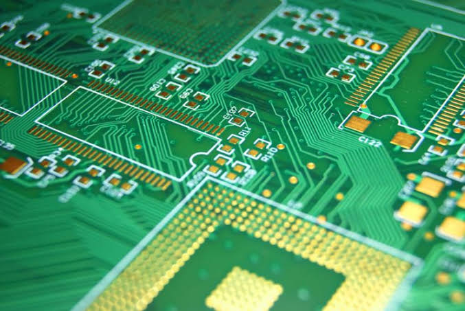
PCB layout engineering requires careful consideration of several factors to ensure the final board meets performance, manufacturability, and reliability standards.
.jpg)
Functionality: Components should be placed in a way that aligns with the signal flow, allowing for efficient routing and minimizing the distance between related components.
Accessibility: Components that need regular maintenance or testing should be easy to access on the board.
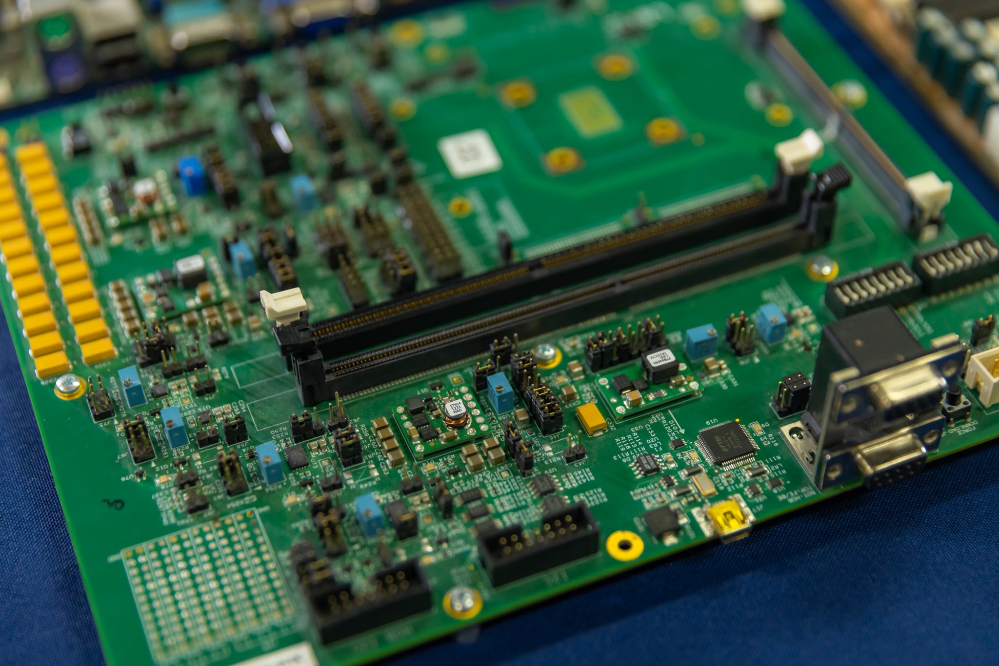
Components that generate heat, such as power transistors or voltage regulators, should be placed in areas with sufficient space or near heat sinks to ensure proper heat dissipation.
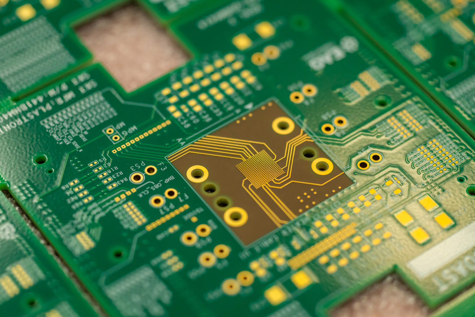
Signal Traces: Signal traces should be as short and direct as possible to minimize resistance, inductance, and capacitance.
Trace Width and Spacing: Proper trace width and spacing are critical for both electrical performance and manufacturability to avoid short circuits.
Partner with Altest Corporation for your next high-reliability PCB fabrication and turnkey SMT assembly project. Our engineering team is ready to review your gerber files and provide a detailed, competitive estimate.