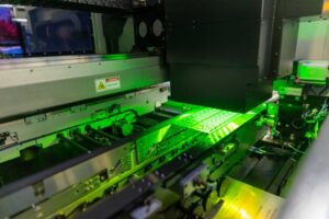
Automated Optical Inspection (AOI) is another crucial non-destructive testing (NDT) method used in manufacturing and quality control. Unlike 3D X-ray testing, which uses X-rays to examine the internal structure of objects, AOI uses high-resolution cameras and computer algorithms to visually inspect the external surfaces of components and assemblies.
At Altest Corporation in San Jose, CA, AOI testing would likely be employed for inspecting the external quality of various products, especially in industries like electronics, automotive, and medical devices. Here’s how AOI works, its applications, and how it could be utilized by Altest Corporation.
Automated Optical Inspection involves the following key steps:
High-resolution cameras (often using visible light or sometimes infrared light) capture detailed images of the surface of an object, typically a printed circuit board (PCB) or a component.
These images are processed by sophisticated software algorithms that can analyze the captured images in real time. The software compares the actual appearance of the object to pre-defined models or specifications (CAD files, design rules, or standards).
The system looks for discrepancies, such as:
Based on the analysis, the system provides a pass or fail result, and can also flag areas for further manual inspection if needed.
AOI is widely used in industries where precision and reliability are critical, particularly in:
AOI is especially useful in PCB assembly for detecting soldering defects, incorrectly placed components, missing components, or broken connections.
AOI systems can inspect components like wiring harnesses, LED assemblies, and mechanical parts to ensure that they are defect-free before assembly.
Medical device manufacturers use AOI to ensure that the surface finishes, component placements, and assembly integrity of devices like catheters, implants, or surgical instruments meet stringent quality standards.
AOI can be used to ensure that products like batteries, small mechanical devices, or consumer electronics are free from manufacturing defects.
AOI is much faster than manual inspection, allowing for real-time feedback and quicker detection of defects, which is critical in high-volume manufacturing environments.
The automated nature of AOI ensures that inspections are consistent across the entire production run, reducing human error and variability.
AOI systems can detect minute defects with incredible accuracy, including very small soldering issues, surface imperfections, or minor misalignments that would be hard for the human eye to detect.
While AOI systems may require an initial investment in equipment, they can significantly reduce labor costs associated with manual inspection, and they can operate 24/7 without fatigue.
AOI is entirely non-destructive, meaning the components or assemblies being tested can be re-used or moved to the next stage of production without any damage.
At Altest Corporation in San Jose, CA, AOI testing would likely be a critical part of their quality assurance and failure analysis services. Their services could include:
Altest may use AOI to inspect products in high-volume production lines, ensuring that any defects are caught early in the process. This helps to prevent faulty components from moving forward to later stages of production or reaching customers.
For customers who are in the prototype development phase, Altest can use AOI to help quickly identify design flaws or manufacturing issues, ensuring that products meet the necessary specifications before mass production.
In electronics, solder joint inspection is a primary application of AOI. Altest may employ AOI systems to examine solder joints for cold soldering, solder bridges, insufficient solder, or incorrect component placement.
Altest’s AOI solutions can automate the visual inspection process, allowing them to deliver high-throughput, error-free quality checks for customers in industries like electronics, automotive, and medical devices.
Captures a flat image of the object and analyzes it. It’s typically used for detecting surface defects or component misplacement.
Uses advanced technologies such as laser triangulation or stereo vision to capture the height profile of a component, enabling detection of soldering defects (such as solder bridges or insufficient solder) and component height issues.
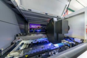
By identifying defects early in the process, AOI can help prevent delays caused by defective products being caught late in the manufacturing process.
With AOI, customers can ensure the quality of their products by detecting defects early, leading to improved overall product reliability and customer satisfaction.
Detecting defects in real-time minimizes the need to scrap entire batches of products, saving money and resources in the long run.
Frequently Asked Questions About AOI Testing
Automated Optical Inspection (AOI) testing is a non-destructive inspection method that uses high-resolution cameras, lighting, and computer software algorithms to visually inspect components and assemblies. In PCB manufacturing, AOI testing is used to identify defects such as missing components, component misalignment, soldering defects, incorrect component placement, and orientation errors.
AOI testing works by capturing high-resolution images of a PCB or component using cameras and analyzing those images with specialized software. The system compares the actual appearance of the PCB with predefined models, CAD files, design rules, or specifications to identify potential defects. The AOI system then provides a pass or fail result and can flag areas that require further inspection.
AOI testing can detect a wide range of PCB defects, including component misalignment, missing components, incorrect component placement, soldering defects, solder bridges, cold solder joints, insufficient solder, package orientation errors, broken connections, scratches, and other surface imperfections.
AOI testing is important for PCB assembly because it helps identify manufacturing defects early in the production process. Automated inspection provides consistent and accurate quality checks, helping manufacturers prevent defective PCBs from moving to later production stages and improving overall PCB quality and reliability.
2D AOI captures a flat image of the PCB or component and analyzes it to identify surface defects, component placement problems, and other visual issues. 3D AOI uses technologies such as laser triangulation or stereo vision to capture the height profile of components, providing additional information for detecting soldering defects, solder bridges, insufficient solder, and component height issues.
Yes. AOI testing can detect various soldering defects during PCB assembly. These may include cold solder joints, solder bridges, insufficient solder, and other solder-related issues. AOI systems inspect solder joints visually and compare them against predefined specifications.
Automated Optical Inspection can detect defects including missing components, incorrectly placed components, component misalignment, incorrect component orientation, solder bridges, cold solder joints, insufficient solder, broken connections, scratches, and other surface or assembly defects.
AOI testing services are used across industries where precision, reliability, and quality control are important. These include electronics and PCB manufacturing, automotive, medical devices, consumer electronics, and other manufacturing applications where components and assemblies require accurate inspection.
Yes. AOI testing is a non-destructive testing method. The inspection process does not damage the components or assemblies being tested, allowing products that pass inspection to be reused or moved to the next stage of production.
AOI testing provides several benefits for PCB manufacturing, including faster inspection, consistent quality control, high inspection accuracy, reduced human error, early defect detection, and reduced labor requirements. AOI systems can also opera
Counterfeit Authentication Testing is a critical service used to verify the authenticity of electronic components and products to protect manufacturers, suppliers, and consumers from counterfeit or substandard parts. Counterfeit parts can pose serious risks in industries such as aerospace, automotive, medical devices, and consumer electronics, where product reliability and safety are paramount. Altest Corporation in San Jose, CA, likely offers counterfeit authentication (authenticity) testing as part of its quality assurance and failure analysis services to help businesses prevent and detect counterfeit components.
Here’s an overview of counterfeit authentication testing, how it works, and how Altest Corporation might use it to support customers:
Counterfeit authentication testing is a process designed to confirm whether a component, device, or product is genuine or counterfeit. This testing can involve a combination of visual inspections, advanced analytical techniques, and functional testing to detect anomalies that may indicate counterfeiting, such as unauthorized modifications, inferior materials, or substandard manufacturing practices.
Counterfeit authentication testing typically involves several stages and techniques, depending on the type of component being tested and the methods used by counterfeiters. Below are the key components of the process:
Counterfeit authentication testing is particularly important in industries where high-performance, safety-critical components are used, and the risks of counterfeit parts are high. Some key industries where counterfeit authentication testing is crucial include:
Counterfeit components in aircraft systems can endanger passenger safety. Authentication testing ensures that avionics, power systems, and control systems are free from counterfeit parts.
Counterfeit automotive parts, such as sensors, microcontrollers, or engine control units (ECUs), can lead to vehicle malfunctions, increased repair costs, or even accidents. Counterfeit authentication testing helps ensure vehicle safety and regulatory compliance.
Counterfeit medical components, such as pacemakers, diagnostic devices, and implantable devices, can have life-threatening consequences. Counterfeit authentication testing is vital in ensuring patient safety and regulatory compliance.
Counterfeit semiconductors, memory chips, and components used in smartphones, computers, and other consumer devices can lead to product failures, data breaches, or damage to customers’ devices.
Counterfeit parts in defense systems (e.g., in radar, communications, weapons, or guidance systems) could have disastrous consequences. Testing helps maintain the integrity of defense technologies and national security.
The primary benefit of counterfeit authentication testing is that it helps detect counterfeit parts before they are integrated into products, preventing safety hazards, product failures, and costly recalls.
Many industries, especially aerospace, automotive, and medical devices, have strict regulations (e.g., ISO 9001, AS9100, or FDA standards) that require proving the authenticity of parts used in manufacturing. Authentication testing helps ensure compliance with these regulations.
Manufacturers are increasingly concerned with maintaining their brand reputation and protecting their customers from counterfeit goods. By performing authentication testing, manufacturers can ensure that only genuine parts are used, safeguarding both their reputation and customer trust.
Early detection of counterfeit parts helps reduce costs related to product failures, warranty claims, recalls, or reputational damage. It can also prevent the further distribution of substandard or unsafe products.
Authentication testing helps create traceable records of each part’s authenticity, enabling manufacturers and end-users to track the source of counterfeit parts if they are found in the supply chain.
Altest Corporation, based in San Jose, CA, would likely provide comprehensive counterfeit authentication testing services for a variety of industries. Their offerings could include:
Altest may offer a range of testing techniques, from visual inspections and X-ray imaging to material analysis and functional testing, to ensure the authenticity of parts and devices.
Altest might conduct audits of the customer’s supply chain, identifying potential sources of counterfeit parts and recommending actions to ensure that only authentic components are sourced.
If a counterfeit part is detected, Altest can perform failure analysis to determine the cause of failure and the potential risks associated with using counterfeit components. This could include analyzing electrical properties, materials, or reverse engineering.
Depending on customer needs, Altest may design specific counterfeit testing protocols tailored to the type of product, such as specialized testing for semiconductors, PCBs, or medical devices.
After performing counterfeit authentication testing, Altest would provide detailed test reports and certifications, which help businesses comply with industry standards and demonstrate due diligence in ensuring product authenticity.
Frequently Asked Questions About Counterfeit Authentication Testing
Counterfeit authentication testing is a process used to verify whether an electronic component, device, or product is genuine or counterfeit. Counterfeit component testing can involve visual inspection, advanced analytical techniques, electrical testing, X-ray inspection, and material analysis.
Counterfeit authentication testing typically involves multiple inspection and testing methods, including visual inspection, microscopy, X-ray inspection, electrical testing, chemical and material analysis, die analysis, microsectioning, and reverse engineering. The testing methods used depend on the type of electronic component being evaluated.
Counterfeit electronic components can be detected by examining markings, packaging, surface features, internal structures, electrical performance, material composition, and die characteristics. These inspections help identify differences between suspected counterfeit components and authentic parts.
Common counterfeit component testing methods include visual inspection, microscopy, X-ray inspection, electrical testing, X-ray fluorescence (XRF), Scanning Electron Microscopy (SEM), Energy Dispersive X-ray Spectroscopy (EDS), die analysis, microsectioning, and reverse engineering.
Counterfeit component testing is the process of examining electronic components to determine their authenticity and identify unauthorized modifications, inferior materials, substandard manufacturing, or other characteristics associated with counterfeit parts.
Yes. X-ray inspection can examine the internal structure of electronic components and help identify anomalies such as incorrect die bonding, misaligned internal components, missing connections, or other differences when compared with known good parts.
Electrical testing evaluates the performance of an electronic component under specified operating conditions. It can identify characteristics outside the required range, including differences in resistance, voltage, current behavior, voltage thresholds, and current leakage.
Counterfeit authentication testing is important for industries such as aerospace, automotive, medical devices, consumer electronics, military, and defense. These industries rely on reliable, authentic components where safety, performance, and product reliability are critical.
Counterfeit parts testing helps detect counterfeit electronic components before they are integrated into products. Early detection can help prevent product failures, safety hazards, costly recalls, warranty claims, and reputational damage.
Counterfeit authentication testing helps identify potentially counterfeit components and create traceable records of component authenticity. This can help manufacturers and end-users identify potential sources of counterfeit parts within the supply chain and support better quality control.
In today’s electronics manufacturing industry, where precision and reliability are paramount, Flying Probe Testing (FPT) has emerged as an invaluable tool for PCB quality assurance. Flying probe testing services provide flexible, high-accuracy testing of printed circuit boards (PCBs), allowing manufacturers to identify and correct potential faults in assembled boards before they reach consumers.
This article discusses the mechanics of flying probe testing, its benefits, and its role in modern electronics manufacturing.
Flying probe testing is a method of testing PCBs that employs moving probes to inspect each node (test point) on a board without requiring fixed test fixtures.
Unlike traditional In-Circuit Testing (ICT), which uses a bed-of-nails fixture to make connections, FPT uses a series of robotic arms or probes that “fly” across the PCB. These probes make contact with specific points on the board to test for:
The lack of a fixed test fixture makes flying probe testing ideal for low- to medium-volume production runs, prototypes, and complex PCBs.
With its flexibility and high precision, flying probe testing is widely used in industries that prioritize quality, including:
Flying probe testing involves several key steps to inspect and verify the electrical performance of a PCB.
The FPT system is programmed to identify the specific locations on the PCB that need to be tested. It is loaded with the board’s layout data, including component locations and expected electrical characteristics.
Robotic probes move across the PCB at high speed, contacting each test point as programmed. The test probes can access densely packed boards and are often configured to reach both the top and bottom sides of a PCB.
The probes check for electrical continuity, resistance, capacitance, and other parameters. Some systems can also test diode polarity, transistor orientation, and other component-specific properties.
Once testing is complete, the FPT system generates a report identifying any faults detected on the board. Engineers can then analyze the data to diagnose and rectify issues before the PCB moves on to the next stage of production.
Unlike ICT, flying probe testing requires no custom test fixture. This reduces setup costs and lead times, especially for low-volume or prototype production runs.
The flying probes can also be reprogrammed quickly, allowing manufacturers to make efficient changes between different PCB designs.
Flying probe systems can handle a wide range of PCB layouts and complexities, from single-sided boards to multi-layer, densely packed designs.
This flexibility is particularly valuable for manufacturers working with prototypes or frequently changing product lines.
For small production runs, the cost of creating a dedicated test fixture for ICT may be prohibitive.
Flying probe testing provides a cost-effective solution by eliminating fixture costs and allowing manufacturers to test smaller production batches efficiently.
Advanced flying probe testers are capable of measuring very fine pitches and testing complex configurations.
With precise robotic movement and intelligent programming, these systems can identify subtle defects that may be missed by other testing methods.
During the prototype stage, PCB designs may undergo frequent changes. Flying probe testing provides rapid adaptability, allowing manufacturers to quickly adjust test programs for new PCB revisions.
This helps expedite the testing and development cycle.
For electronics companies developing new products, flying probe testing is ideal for testing prototypes quickly and effectively.
As new designs are introduced, FPT can adapt to each iteration without requiring a new fixture. This allows manufacturers to identify and resolve issues early in the development cycle.
Flying probe testing is suitable for manufacturers producing low to medium quantities, such as specialized or niche electronics.
These manufacturers benefit from the lower cost and flexibility of FPT because it eliminates the need to invest in fixed test fixtures.
For production environments that handle various PCB designs, flying probe testing provides the ability to switch quickly between jobs.
This makes FPT ideal for contract manufacturers serving multiple customers with different PCB designs.
Advanced, high-density PCBs with multiple layers, intricate vias, and fine-pitch components require precise testing.
Flying probe testing provides the accuracy needed to test these intricate designs, helping ensure reliability and performance in demanding applications such as aerospace and medical devices.
Modern flying probe systems are designed to operate at higher speeds, with some models using multiple probes per side.
This allows for parallel testing, significantly reducing testing time and increasing production throughput.
Many modern FPT systems include sophisticated software that enables:
With machine learning capabilities, some systems can learn from previous testing data, improving accuracy and diagnostic capabilities over time.
As PCBs become increasingly complex, some flying probe systems incorporate 3D imaging and Automated Optical Inspection (AOI) capabilities.
This hybrid approach allows for more comprehensive testing, including measurements of solder joint quality and component positioning.
Some flying probe systems offer additional capabilities such as thermal profiling and high-voltage testing.
These capabilities are essential for products operating under extreme conditions, including automotive and industrial applications.
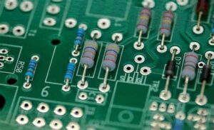
Through-Hole Assembly (also known as Through-Hole Technology or THT) is a type of electronic assembly process in which components with leads (or pins) are inserted into holes drilled through a printed circuit board (PCB) and soldered on the opposite side. This is one of the traditional methods of mounting electronic components and is particularly well-suited for components that require a more robust mechanical connection, or for applications that involve heavy-duty components, power devices, or high-stress environments.
While Surface-Mount Technology (SMT) has largely replaced through-hole in modern electronics, through-hole assembly is still essential in many industries where component reliability, thermal performance, or the need for higher mechanical strength is critical.
Through-hole assembly is a multi-step process that includes component insertion, soldering, inspection, and testing. Here’s an overview of each step in the process:
Before the components can be inserted into the PCB, the PCB itself must be prepared.
Once the PCB is prepared, the next step is inserting the components. Through-hole components have leads that go through the holes in the PCB.
In small-scale or low-volume production, manual insertion may be used. Workers manually insert each component through the correct hole in the PCB, bending the leads on the opposite side to hold the components in place.
After insertion, the component leads may need to be bent or trimmed. Lead bending machines are used for this step, particularly in automated environments, to ensure the leads are in the right position for soldering.
Once the components are inserted and the leads are secured, the next step is soldering. There are two main methods for soldering through-hole components: wave soldering and hand soldering.
For mixed-technology boards (combining both through-hole and surface-mount components), selective soldering is used. This method involves using a soldering iron or a robotic arm to selectively apply solder only to the through-hole component leads, avoiding the surface-mount areas.
After soldering, the PCB undergoes additional steps to ensure the assembly is clean, functional, and free from defects.
After the soldering process, thorough functional testing is performed to ensure the board operates correctly. This step includes:
After testing, the PCB undergoes a final inspection to ensure it meets quality standards.
A final visual inspection ensures all components are properly inserted and soldered, and that there are no visible defects like misaligned components, solder bridges, or mechanical damage.
Rigid Board Assembly refers to the process of assembling electronic components onto a rigid PCB (Printed Circuit Board), which is a non-flexible, solid substrate used to support and electrically connect components such as resistors, capacitors, integrated circuits (ICs), and connectors. Unlike flexible or rigid-flex boards, rigid PCBs maintain their shape and are typically used in a wide range of electronic devices and applications, from consumer electronics to industrial equipment.
The assembly of rigid PCBs is a multi-step process involving several key stages, including design, fabrication, component placement, soldering, and testing.
Before the assembly process begins, the PCB design must be finalized. This step is essential for creating a functional and manufacturable rigid board.
The BOM specifies the components to be used, including resistors, capacitors, ICs, and connectors, and is used for sourcing parts.
After the design is finalized, fabrication files are generated (such as Gerber files and NC drill files) for the PCB manufacturer to produce the rigid PCB.
The PCB fabrication process creates the physical rigid board according to the design files. The key steps in this process include:
Rigid PCBs are typically made from fiberglass (such as FR4), which is a durable, non-flexible material that provides mechanical strength and electrical insulation.
Other materials like CEM-1 or CEM-3 are sometimes used for specific applications.
For multi-layer boards, the process involves stacking several layers of conductive and insulating materials, which are then laminated together using heat and pressure.
The inner layers of the PCB (for multi-layer designs) are often created by etching copper onto a substrate and then bonding them with additional layers.
A thin layer of copper foil is laminated onto the board, and then the unwanted copper is removed via an etching process. This creates the conductive traces that will carry the electrical signals.
The surface of the PCB is treated with a finish to protect the copper and improve solderability. Common finishes include HASL (Hot Air Solder Leveling), ENIG (Electroless Nickel Immersion Gold), or OSP (Organic Solderability Preservative).
After the PCB is fabricated, the next step is to source the components and place them onto the board. This process typically includes:
Soldering is the process that permanently attaches the components to the PCB by forming electrical connections through melted solder. The main soldering methods used in rigid board assembly include:
In cases where automatic methods are not feasible or for small production runs, hand soldering with a soldering iron may be used, particularly for small or delicate components.
Once soldering is complete, it’s critical to ensure that the PCB assembly is functional and free from defects. This involves several stages of inspection and testing:
ICT tests the functionality of the individual components and checks for shorts, opens, and other faults. It involves applying test signals to the circuit and verifying that the outputs match the expected results.
After ICT, functional testing is performed to verify that the entire PCB assembly works as intended in the real-world application. This may involve testing the board with power applied and running through its intended use cases.
For boards with fine-pitch components (e.g., BGAs) or multi-layer structures, X-ray inspection can be used to check the internal solder joints and vias for defects that are not visible on the surface.
After testing and inspection, the PCB is cleaned to remove any flux residues, soldering debris, or other contaminants that could affect performance or longevity.
Before the assembled PCBs are shipped to the customer or integrated into the final product, they undergo a final inspection to ensure they meet quality standards.
Rigid PCBs are widely used across many industries and applications, including:
System Integration and Box Build Assembly refers to the process of assembling and integrating complex electronic systems within a protective enclosure or box. This includes not only assembling the electronic components onto a printed circuit board (PCB), but also incorporating those PCBs into a larger system, connecting various subsystems (such as power supplies, connectors, sensors, switches, displays, etc.), and ensuring the final product is properly housed in a box or enclosure for protection, usability, and functionality.
Box build assembly typically involves the integration of hardware, software, and mechanical elements, creating a fully functional system or product. This process is crucial for industries like consumer electronics, automotive, industrial equipment, medical devices, telecommunications, and aerospace, where end products are often complex systems that require both electronic and mechanical assembly.
The system integration and box build assembly process generally includes several stages: Design and Engineering, Assembly of the Electronics, Mechanical Assembly, System Integration, Testing and Quality Assurance, and Final Packaging. Below is a detailed breakdown of each stage:
The first step in the box build process is to design the overall system architecture, including both the electronics and the mechanical aspects.
System Design and Requirements
Once the design is complete, the assembly of the electronic components begins. This step typically includes the SMT (Surface-Mount Technology) assembly of the PCB, followed by the integration of the PCB with the other system components.
PCB Assembly (SMT and Through-Hole Components)
This phase involves the assembly of the mechanical parts of the system, including the enclosure and any external components. This is often done in parallel with the electronic assembly.
This is the phase where all parts of the system come together. It involves both the electrical integration and the mechanical integration of the components.
If the system includes programmable components (e.g., microcontrollers, FPGAs), the firmware or software is loaded onto the devices, and the system is configured for its intended operation.
Comprehensive testing is crucial to ensure the system operates as intended. Testing verifies both the electrical performance of the system and its mechanical integrity.
The system may need to meet specific industry standards or regulatory requirements, such as CE, UL, or RoHS certifications, depending on the product type and target market.
Once the system has passed all tests and quality checks, it is ready for final packaging.
System integration box build assemblies are used in a wide variety of industries and applications, including:
Surface-Mount Technology (SMT) Assembly is the process of assembling electronic components directly onto the surface of a printed circuit board (PCB) without the need for through-holes. In SMT, the components are typically small and are mounted on the surface of the PCB using solder paste and reflow soldering. This process is highly automated, efficient, and suitable for high-volume manufacturing of compact and reliable electronic devices.
The SMT assembly process involves several stages: solder paste application, component placement, reflow soldering, and inspection and testing. Here’s an overview of each stage:
The first step in SMT assembly is the application of solder paste to the PCB. Solder paste is a mixture of small metal solder balls (usually made of tin, silver, and copper) suspended in a flux medium. The paste serves both to hold the components in place and to form the solder joints once heated.
Once the solder paste is applied, the next step is the placement of surface-mount components (SMDs) onto the PCB. Components can include resistors, capacitors, integrated circuits (ICs), connectors, and LEDs, all of which are small and designed to be mounted on the surface of the PCB.
Pick-and-Place Machines: These automated machines are used to pick up the components from reels or trays and place them onto the correct locations on the PCB.
Vacuum Grippers: The pick-and-place machine uses vacuum suction to pick up the components and place them accurately on the pads covered with solder paste.
Placement Accuracy: These machines are highly precise, capable of placing components with tolerances of a few mils (thousandths of an inch). This is essential for handling very fine-pitch components like BGAs (Ball Grid Arrays) or QFNs (Quad Flat No-leads).
Component Orientation: For polarized components (like diodes or electrolytic capacitors), the machine ensures they are oriented correctly according to the PCB design.
Component Size: SMT is ideal for small, lightweight components, typically ranging from 01005 (the smallest size) to components with large thermal dissipation like power transistors.
Placement Speed: High-speed pick-and-place machines are capable of placing thousands of components per hour, making the process efficient for high-volume production.
Precision: The placement accuracy is crucial for ensuring reliable solder joints and preventing defects such as misalignment or tombstoning (when a component stands upright due to uneven soldering).
After the components are placed, the PCB is passed through a reflow soldering oven, where the solder paste is melted to form solid solder joints between the PCB pads and the component leads.
Preheat Zone: The PCB is heated gradually in the preheat zone to avoid thermal shock and to activate the flux in the solder paste. This zone prepares the board for the reflow stage.
Reflow Zone: The PCB enters the reflow zone, where the temperature is raised to the melting point of the solder paste (typically around 220-250°C). This causes the solder to melt and form a bond between the component leads and the PCB pads.
Cooling Zone: After the solder is melted, the board is gradually cooled, allowing the solder to solidify and form reliable solder joints.
Temperature Profile: The reflow soldering process requires a carefully controlled temperature profile to ensure that the components and solder paste heat evenly. Too high a temperature can damage components, while too low a temperature may result in insufficient soldering.
Solder Joint Quality: Proper reflow soldering results in well-formed solder joints that are both mechanically strong and electrically conductive.
After reflow soldering, the assembled PCB is thoroughly inspected and tested to ensure that all components are correctly soldered and that the board functions as expected.
AOI is used to automatically check for defects in the solder joints, component placement, and alignment. It captures high-resolution images of the board and compares them to a predefined template to identify common issues like:
Solder bridges
Missing components
Misaligned components
Insufficient or excessive solder
Benefits: AOI is fast, non-destructive, and can detect issues that are invisible to the naked eye, such as micro-solder bridges or fine-pitch misalignments.
For more complex PCBs with hidden or non-visible solder joints (such as those under BGAs or QFNs), X-ray inspection is used to check the quality of the solder joints.
X-ray inspection helps to detect issues like:
Insufficient solder
Voids (air pockets) in the solder joint
Cold solder joints
BGA solder ball defects
Functional testing ensures that the finished PCB performs as expected in its intended application. This may involve:
Applying power and checking for correct voltages
Signal testing and functional checks (e.g., communication protocols, signal integrity)
Automated tests or manual tests (e.g., using oscilloscopes or multimeters) are performed to verify the PCB’s functionality.
After successful inspection and testing, the PCB undergoes a final quality check to ensure that all aspects of the assembly are correct.
If necessary, the PCB is cleaned to remove any flux residue left from the soldering process. Ultrasonic cleaning or brush cleaning with solvents may be used to ensure the board is free from contaminants.
The final PCB assemblies are carefully packaged to avoid damage during transport. Anti-static bags, trays, or tubes are often used to protect the boards from electrostatic discharge (ESD) and physical damage.
Higher Component Density: SMT allows for smaller components and higher component density, leading to more compact and lightweight PCBs.
Improved Reliability: SMT components tend to have better mechanical and thermal properties compared to through-hole components, leading to improved reliability.
Automated Process: SMT assembly is highly automated, allowing for high-speed production with minimal human intervention, which is ideal for mass production.
Lower Costs: The automated nature of SMT reduces labor costs and material waste, making it cost-effective for large production runs.
Flexibility: SMT can be used for both low and high-volume production and is suitable for a wide variety of component types (e.g., resistors, capacitors, ICs, LEDs).
SMT is widely used in the assembly of electronic products across many industries, including:
Consumer Electronics: Smartphones, laptops, tablets, TVs, and gaming consoles.
Automotive: Electronic control units (ECUs), infotainment systems, sensors, and power management systems.
Medical Devices: Diagnostic equipment, wearable devices, and imaging systems.
Industrial Equipment: PLCs (Programmable Logic Controllers), robotics, and industrial control systems.
Aerospace and Military: Avionics, communications systems, and radar.
Repair and rework assembly is an essential process in PCB manufacturing and electronic assembly. It helps correct manufacturing defects, replace faulty components, repair damaged PCB traces, and improve overall product quality. Whether you’re working with SMT, through-hole, or BGA assemblies, repair and rework ensure printed circuit boards meet quality and performance standards. Below is a detailed guide explaining the repair and rework assembly process.
Repair and rework assembly refers to the processes used to fix defects, correct errors, or modify a printed circuit board (PCB) or electronic assembly after it has been manufactured. This is common in electronics production, as it’s rare for every unit to be perfect, especially when dealing with complex circuits, high-density designs, or issues that arise during soldering and component placement.
The process of fixing a specific issue, such as a damaged trace, component, or connection, on an already assembled PCB. It may involve removing damaged parts, replacing them, or repairing traces or solder joints.
The act of correcting or modifying a PCB after it has been assembled but before it’s considered fully functional or finalized. Rework can involve things like adjusting solder joints, replacing components, or adding additional elements to correct an issue or improve performance.
The repair and rework process can involve several different techniques depending on the nature of the problem and the type of assembly. Here are some of the primary methods used:
Objective: Identify defects like solder bridges, cold solder joints, missing components, or incorrect component placement.
Tools: Magnification tools (like microscopes), visual inspection systems (automated optical inspection, or AOI), and manual checklists.
Common Defects: Broken traces, incorrect component orientation, soldering issues, or component damage.
Objective: Remove faulty or unwanted components from the PCB.
Soldering Iron: Used to heat the solder joints and remove components by hand. This is the most common method for desoldering components like resistors, capacitors, or chips.
Desoldering Pump: A hand-held tool that uses suction to remove melted solder from joints.
Desoldering Braid: A woven copper braid that absorbs molten solder when heated with a soldering iron, leaving the joint clear.
Considerations: Care must be taken not to damage the PCB or surrounding components during desoldering.
Objective: Fix soldering problems like cold joints, insufficient solder, or bridges (short circuits).
Reflow Soldering: Involves using a reflow oven or a hot air rework station to melt solder paste and reflow it to form the correct joint. This is often used for surface-mount components (SMDs).
Hand Soldering: For smaller-scale fixes or through-hole components, a soldering iron is used to manually correct joints.
Hot Air Rework: Hot air is directed to a specific area to reflow solder paste and components, often used for SMD components that need to be replaced or repositioned.
Objective: Remove defective components and replace them with new ones.
Identify the defective component through testing or visual inspection.
Desolder the faulty component.
Solder a new component in place, making sure it is oriented and positioned correctly.
Special Consideration: Some components, especially those with sensitive leads or fine-pitch connections (like BGAs or fine-pitch QFNs), may require more precise handling using tools like soldering stations, reflow ovens, or hot air guns.
Objective: Fix traces that are broken or pads that are lifted or damaged during manufacturing or testing.
Wire Jumpers: In cases where a trace is damaged, a jumper wire can be soldered to bypass the damaged area and re-establish the connection.
Conductive Ink: Special conductive ink or adhesive can be used to restore connections on the PCB, often in minor repairs.
Trace Rerouting: If a trace is broken and cannot be repaired with a jumper, the trace may be rerouted by cutting the PCB and applying a new route using conductive materials.
Objective: Ensure that components are placed correctly, especially for polarized components like diodes, capacitors, and integrated circuits.
Repositioning Components: For misplaced components, the component is desoldered, and the correct placement is ensured before resoldering.
Component Marking: Components such as capacitors or diodes may need to be replaced in the correct orientation (positive and negative sides). If they are misoriented, rework is necessary to ensure proper polarity.
Objective: After repair or rework, cleaning ensures that no flux residues, solder balls, or other contaminants remain on the board.
Flux Removal: Cleaning solutions or brushes are used to remove flux residues.
Ultrasonic Cleaning: An ultrasonic bath can clean the entire board to remove small particles that are difficult to remove manually.
Air Blower/Brush: Used to remove excess solder or flux from the board after rework.
Objective: After the repair or rework is completed, the PCB must be tested to ensure that the problem has been fixed and that the board works as expected.
Visual Inspection: To ensure the repair work looks correct.
Functional Testing: To ensure the electrical performance is as expected, which may include checking voltage, current, and signal paths.
Automated Optical Inspection (AOI): A machine-based system that inspects the board after rework for missing or misaligned components and soldering defects.
In-circuit Testing (ICT): Checks the integrity of the board and individual components in a more thorough, automated fashion.
Solder Bridges: Solder that has accidentally connected two adjacent pads, causing a short circuit. Fixed by desoldering and cleaning up the area.
Cold Solder Joints: Joints that are improperly soldered, often resulting in a poor electrical connection. These can be fixed by reflowing the solder or adding more solder to the joint.
Misplaced Components: Components placed in the wrong position or orientation. These are typically fixed by desoldering and repositioning the component.
Component Failure: A component that has failed due to heat, manufacturing defects, or electrical stress. The failed component is removed and replaced with a new one.
Damaged Pads/Traces: Traces that have been damaged or broken during assembly or testing. These are repaired using jumpers, conductive ink, or wire bonding.
Delicate Components: Small components, particularly those with fine-pitch leads or BGAs (Ball Grid Arrays), require specialized equipment and expertise for rework.
PCB Damage: Repeated rework or excessive heat can damage the PCB material itself, potentially leading to delamination or trace damage.
Handling High-Density Boards: As PCBs become more complex with smaller components, the risk of damaging traces, pads, or components during rework increases.
Cost: Extensive repair and rework processes can significantly add to manufacturing costs, especially if the defect is widespread or difficult to address.
Soldering Irons & Soldering Stations: Used for adding and removing solder for component work.
Hot Air Rework Stations: Used for desoldering and soldering surface-mount components.
Desoldering Tools: Includes desoldering pumps, braid, and specialized vacuum tools.
Microscopes or Magnification Tools: Used for inspecting tiny components and connections.
Automated Optical Inspection (AOI) Systems: For detecting soldering defects, missing components, and other assembly issues.
Reflow Ovens: Used for large-scale reflow soldering but can also be used in rework when needed.
Multimeters/ICT Fixtures: Used for testing the electrical integrity of a repaired or reworked board.
Repair and rework assembly plays a critical role in ensuring the quality, reliability, and performance of printed circuit boards and electronic assemblies. From visual inspection and component replacement to PCB testing and validation, every step contributes to delivering high-quality PCB repair and rework services for modern electronic manufacturing.
cable harness assembly is a collection of electrical cables or wires bundled together and organized to transmit power or data within a device or machinery. This assembly is commonly used in various industries, including automotive, aerospace, consumer electronics, and industrial applications. The purpose of the cable harness is to provide a reliable, organized, and efficient way of routing and managing electrical signals or power between components.
Wires or Cables:These are the individual electrical conductors that carry power, signals, or data. They can be made of copper, aluminum, or other conductive materials, and may be insulated or uninsulated, depending on the application.
Connectors:These are used to attach the cable harness to other electrical components, such as sensors, controllers, motors, or power sources. Connectors may be pre-crimped to the wires or be attached during the assembly process.
Insulation or Sleeving: The cables may be covered with insulating materials (e.g., PVC, Teflon, or braided material) to protect them from environmental factors like heat, abrasion, and moisture.
Strain Relief:This is a mechanism used to prevent the cables from being pulled out of the connectors, reducing the risk of damage from physical stress.
Cable Ties or Clips: These are used to bundle the cables together in an organized way, often with a specific layout that minimizes tangling or interference.
Labels orMarkers:These are used to identify each wire or connector within the harness, which makes installation, troubleshooting, and maintenance easier.
Engineering & Planning: Before assembly, engineers design the cable harness according to the requirements of the application. This involves determining the wire types, lengths, connectors, and the layout to ensure that the harness will function properly within the system.
Bill of Materials (BOM):A list of all the components, including wires, connectors, terminals, and other materials needed for the harness.
Cutting and Stripping the Cables:The wires are cut to the required lengths and stripped of their insulation at the ends where connectors or terminals will be attached.
Crimping:The stripped ends of the wires are attached to connectors using crimping tools, which securely press the metal contacts of the connector onto the wire ends.
Soldering:In some cases, wires may be soldered to the connectors or terminals.
Bundling and Organizing:The wires are bundled together using cable ties, clips, or spiral wrap. The bundle may be arranged in a specific pattern to reduce electromagnetic interference (EMI) or to optimize space.
Insulation or Sleeving:Depending on the environmental requirements, the cables are sleeved with heat shrink tubing or other insulating materials. This provides extra protection from heat, abrasion, and chemicals.
Testing and Quality Control:Once the harness is fully assembled, it undergoes electrical testing to check for continuity, short circuits, and proper functionality.
Mechanical tests like pull tests and bend tests may also be conducted to ensure durability and strain resistance.
Final Inspection andPackaging:The harness is inspected to ensure that it meets design specifications and industry standards. It is then packaged for shipment or installation.
Automotive Industry:Cable harnesses are used to interconnect electrical systems within vehicles, such as the engine, lights, and infotainment systems.
Aerospace:They are used in aircraft for controlling various systems, including avionics, electrical power, and communications.
Consumer Electronics:Cable harnesses help organize internal wiring for devices like computers, televisions, and smartphones.
Industrial Machinery: In factories and production lines, cable harnesses provide power and data connections to motors, sensors, and control systems.
Reduced Installation Time: Pre-assembled cable harnesses simplify installation, reducing the need for complex wiring during assembly.
Organization:They keep electrical systems organized, preventing loose or tangled wires that could lead to errors or damage.
Space Efficiency:A well-designed cable harness minimizes the use of space and allows for efficient routing of wires.
Improved Durability:Properly designed and protected cable harnesses are more resistant to wear, vibration, and environmental factors, leading to a longer lifespan of the electrical system.
The design of a flex PCB is similar to that of a rigid PCB, with the added complexity of needing to account for the material’s ability to bend. Engineers use CAD (Computer-Aided Design) software to create the layout, considering aspects like trace routing, component placement, and the board’s overall flexibility requirements.
Designers also consider flex patterns (how the board will fold or bend) and ensure there are no sharp bends that might damage the circuitry.
Flexible Substrate: The base of the flex PCB is a thin, flexible material. Common materials include polyimide (Kapton) and polyester, chosen for their durability, flexibility, and electrical insulation properties.
Conductive Layers: These are typically copper traces that are applied to the flexible substrate using processes such as etching or lamination.
Solder Mask and Finish: A protective solder mask (similar to rigid PCBs) is applied to prevent shorts and corrosion, and the surface finish (like ENIG, HASL, or OSP) is applied to ensure proper soldering.
Single-layer Flex PCB:This is a simple design where only one layer of copper is used for the circuitry.
Multi-layer Flex PCB: For more complex designs, multiple layers of flexible material are stacked and bonded together with adhesive and copper interconnects between layers. This allows for higher component density and more complex circuits.
Fabrication:The fabrication of a flex PCB involves several steps, such as
Copper Cladding: Thin copper foil is laminated onto the flexible substrate
Etching:The copper is etched away in certain areas to form the desired circuit pattern.
Hole Drilling (if necessary): For components that require through-holes, they are drilled into the flexible substrate.
Plating and Lamination: If it’s a multi-layer design, layers are laminated together, and through-hole plating is done to create electrical connections between the layers.
Assembly:Once the flex PCB is fabricated, the assembly process is similar to that of rigid PCB assembly:
Soldering Components: Surface mount technology (SMT) is the most common method for placing components on a flexible PCB. Because the board is flexible, it requires careful handling to avoid damaging the traces or components.
Bending and Testing: If the flex PCB needs to bend, it is tested to ensure that the components stay in place and that the electrical connections remain intact after bending. This might involve some custom handling equipment or fixtures to position the flex PCB correctly during soldering.
Inspection and Quality Control: The finished flex PCB assembly undergoes rigorous testing, including electrical testing (to check for shorts, open circuits, etc.) and mechanical testing (to ensure it can withstand bending or flexing).
Final Packaging: Once the assembly is complete and passes testing, the flexboard is typically packaged in a way that protects it during transportation or further integration. Special care must be taken to avoid stress on the board that could affect its flexibility or integrity.
Flexboard assemblies are used in a variety of applications, particularly where space is at a premium or where components need to conform to a specific shape. Common applications include:
Wearables: Smartwatches, fitness trackers, medical devices
Consumer Electronics: Smartphones, laptops, and tablets (e.g., internal flexible cables or connectors)
Automotive: In dashboards, control systems, or even flexible sensors
Medical Devices: Flexible sensors or diagnostic equipment
Aerospace and Defense: Flexible interconnects in sensors or systems subject to movement or vibration
Benefits of Flexboard Assemblies
Space-Saving: Flex PCBs can be designed to wrap around objects or fit into smaller spaces, allowing for more compact and lightweight devices.
Reliability in Harsh Conditions: They can tolerate vibrations and mechanical stresses better than rigid boards, making them suitable for applications in dynamic environments.
Flexibility: As the name suggests, they can bend and conform to various shapes, which is useful for applications like foldable or wearable electronics.

