

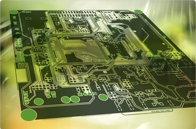
In the rapidly evolving landscape of modern hardware, the physical architecture of a printed circuit board dictates the ultimate success or failure of an electronic product. Professional PCB design services bridge the critical gap between theoretical schematics and physical, manufacturable reality.
At Altest Corporation, our engineering team brings decades of Silicon Valley expertise to every layout project. We understand that as component densities increase and operating frequencies push into the multi-gigahertz range, PCB layout is no longer simply about connecting dots. It is a highly specialized engineering discipline that requires a deep understanding of electromagnetic interference (EMI), signal integrity, thermal dynamics, and strict manufacturing tolerances.
Whether you are a startup developing a revolutionary wearable IoT device, or a Tier-1 defense contractor requiring an ITAR-compliant, high-layer-count communications board, our USA-based PCB design team ensures your intellectual property is protected and your design is optimized for immediate, error-free fabrication and assembly.
The Critical Role of Professional PCB Design Services
Attempting to bypass professional layout engineering often results in catastrophic board failures, costly revision spins, and delayed market entry. A poorly designed PCB might function adequately in a theoretical simulation, but fail entirely when subjected to real-world thermal stress or electromagnetic noise.
Engaging with a dedicated printed circuit board design partner like Altest Corporation provides several core advantages. First, we mitigate parasitic capacitance and inductance that can destroy high-speed digital signals. Second, we implement strategic component placement that naturally isolates noisy analog power supplies from sensitive digital communication buses. Finally, because our design team works directly alongside our manufacturing division, every board we route is inherently designed for maximum manufacturing yield.
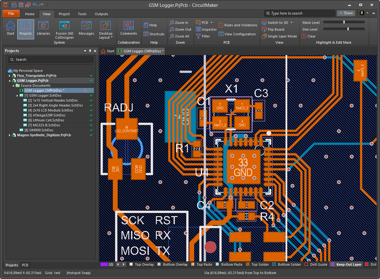
Comprehensive Printed Circuit Board Layout Capabilities
Altest Corporation is equipped to handle the most demanding architectural constraints in the industry. Our comprehensive PCB layout services cover a vast spectrum of technologies, ensuring we can meet the exact specifications of your Bill of Materials (BOM) and mechanical enclosures.
High-Speed Digital PCB Design
Modern data processing requires high-speed communication buses such as PCIe, DDR4/DDR5, USB 3.0, and Gigabit Ethernet. Routing these signals requires extreme precision to maintain signal integrity. Our engineers utilize advanced impedance control calculations, strict length-matching protocols, and differential pair routing to ensure data packets arrive at their destinations without degradation or timing skew. We meticulously manage return paths and solid ground planes to prevent unwanted EMI emissions.
Analog and RF PCB Design
Radio Frequency (RF) and analog circuits are notoriously sensitive to their physical surroundings. Even a millimeter of incorrect trace routing can act as an unintended antenna, ruining a wireless transmission. Our PCB design services include specialized RF layout techniques, such as calculated coplanar waveguides, via stitching for robust RF shielding, and precise isolation techniques to keep analog signals pristine in noisy environments.
High-Density Interconnect (HDI) and Microvias
As consumer electronics and medical devices become progressively smaller, traditional via structures consume too much valuable board real estate. To combat this, we specialize in High-Density Interconnect (HDI) design. By leveraging blind, buried, and laser-drilled staggered microvias, we can route ultra-fine pitch Ball Grid Arrays (BGAs) and dramatically shrink the overall footprint of your PCB without sacrificing electrical performance.
Rigid-Flex and Flex Circuit Design
Mechanical enclosures are no longer limited to simple rectangular boxes. Wearables, aerospace sensors, and folding consumer devices require flexible circuitry that bends without breaking. Designing a flex or rigid-flex PCB introduces complex 3D spacial constraints. Our team meticulously plans the bend radius, staggers traces across flex zones to prevent copper fracturing, and ensures tear-stops are implemented in the polyimide coverlay to guarantee mechanical longevity.
The Altest PCB Design Process: From Concept to Fabrication
Transparency and communication are the bedrocks of our PCB design services. We employ a strict, phase-gated engineering process to ensure your requirements are met at every milestone.
- Schematic Capture and Logic Integration: We begin by translating your electronic concepts into a logical, verified schematic diagram. We run extensive Electrical Rule Checks (ERC) to identify missing connections, floating pins, or power logic errors before physical routing begins.
- Component Footprint Creation and Library Management: An incorrect component footprint will ruin an entire assembly run. Our librarians meticulously create and verify custom CAD decals against the manufacturer's exact datasheet recommendations, ensuring IPC-compliant pad sizes for perfect solder wetting.
- Strategic Component Placement: Before drawing a single trace, we execute a strategic component placement review. We group components by logical function, optimize the placement of decoupling capacitors for maximum effectiveness, and review the layout against your mechanical 3D CAD files (STEP/IGES) to ensure zero interference with the final enclosure.
- Precision Routing and Trace Optimization: Once placement is approved, our engineers execute the physical trace routing. We prioritize critical power distribution networks (PDN) and high-speed data lines, utilizing advanced layer stackups to provide pristine signal return paths.
Design for Manufacturability (DFM) and Design for Testability (DFT)
The most beautiful CAD layout in the world is useless if it cannot be physically manufactured. Because Altest Corporation is a full-service turnkey EMS provider, our layout engineers possess deep knowledge of the physical fabrication and assembly lines.
We bake Design for Manufacturability (DFM) into every layout. This means we naturally avoid common fabrication pitfalls such as acid traps, insufficient annular rings, solder mask slivers, and uneven copper distribution that causes board warpage.
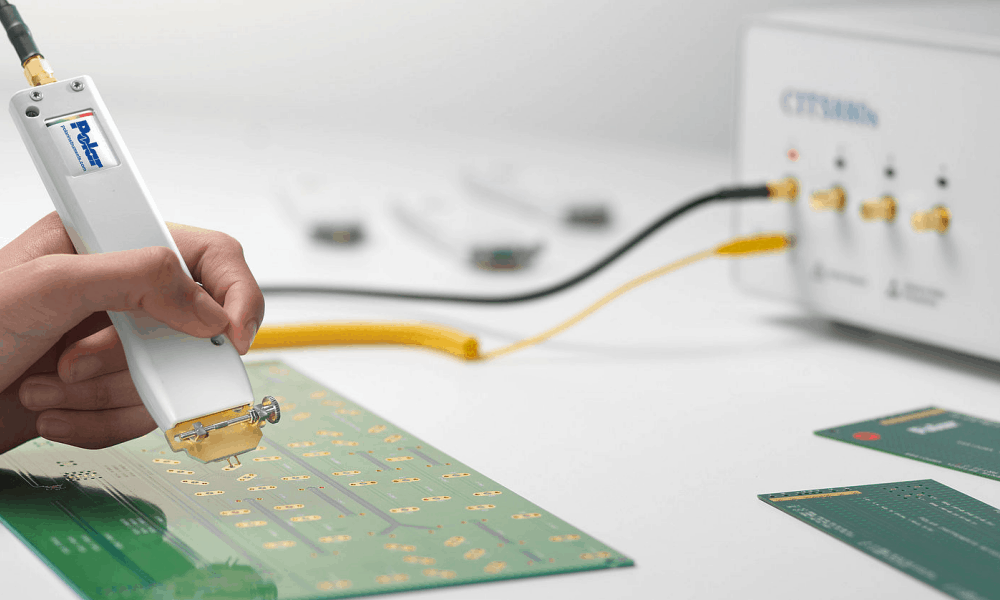
Furthermore, we implement strict Design for Testability (DFT) parameters. By intelligently placing test nodes and via-in-pad test points, we ensure your board can be rapidly and accurately verified on our Flying Probe or In-Circuit Test (ICT) machines during mass production, drastically reducing your total cost of ownership.
Advanced CAD Platforms and Software Mastery
To deliver world-class PCB design services, we utilize industry-leading electronic design automation (EDA) software. Our native fluency in these platforms allows us to seamlessly integrate with your internal engineering teams, accepting and delivering native database files without conversion errors.
- Altium Designer: The industry standard for unified, 3D PCB design.
- Cadence Allegro: The platform of choice for incredibly dense, high-speed enterprise hardware.
- Mentor Graphics PADS: A robust toolset for complex mixed-signal routing.
- Valor NPI: We run final gerber data through Valor NPI software to perform thousands of automated DFM checks before releasing the board to the fabrication facility.
Accelerate Your Product Development Today
Do not let an unoptimized layout bottleneck your time-to-market. Whether you need a simple two-layer prototype or a 32-layer HDI telecommunications backbone, Altest Corporation's USA-based PCB design services team is ready to execute your vision with precision and speed.
Submit Your Schematics for Review