.jpg)
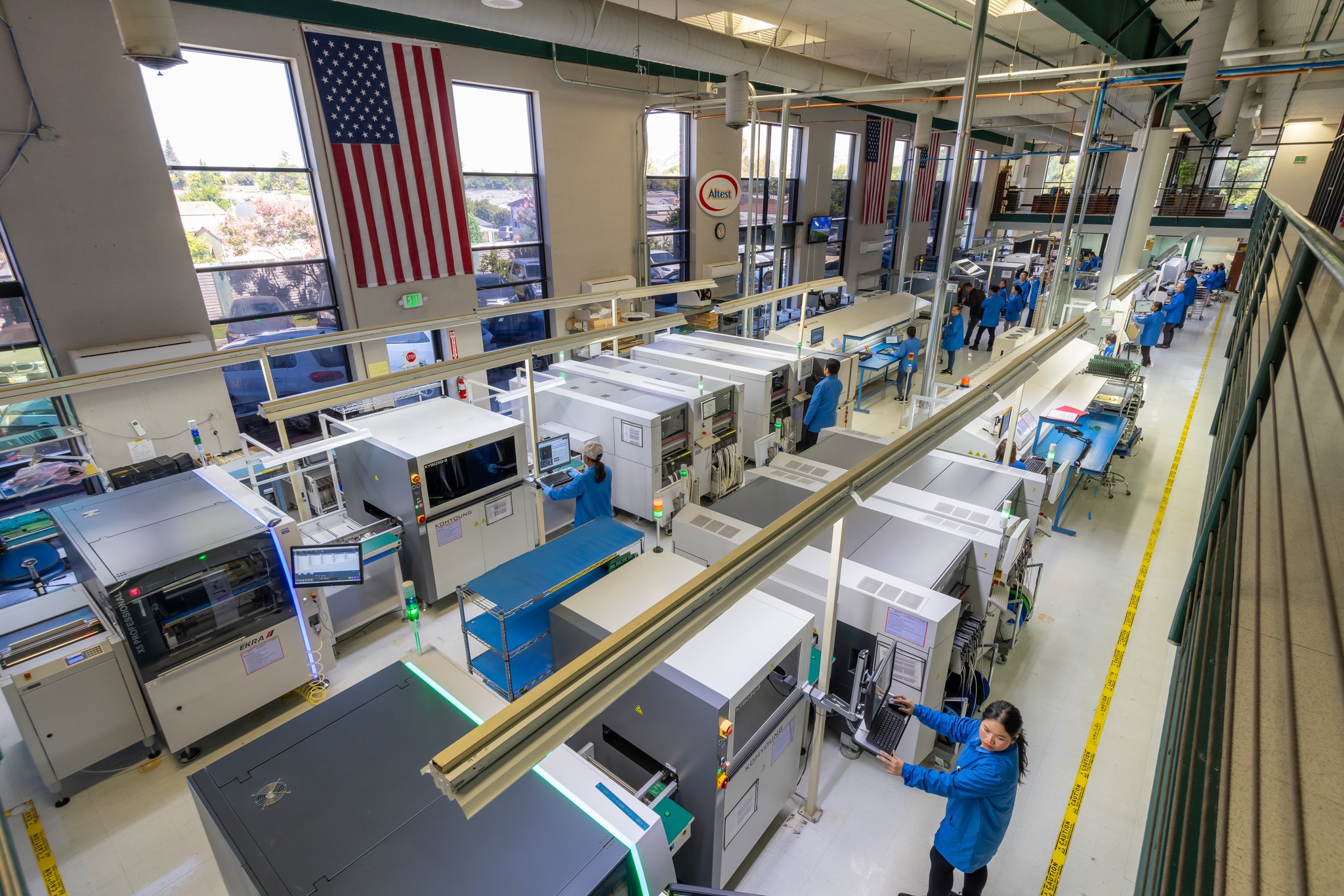
Surface-Mount Technology (SMT) Assembly is the process of assembling electronic components directly onto the surface of a printed circuit board (PCB) without the need for through-holes. In SMT, the components are typically small and are mounted on the surface of the PCB using solder paste and reflow soldering. This process is highly automated, efficient, and suitable for high-volume manufacturing of compact and reliable electronic devices.
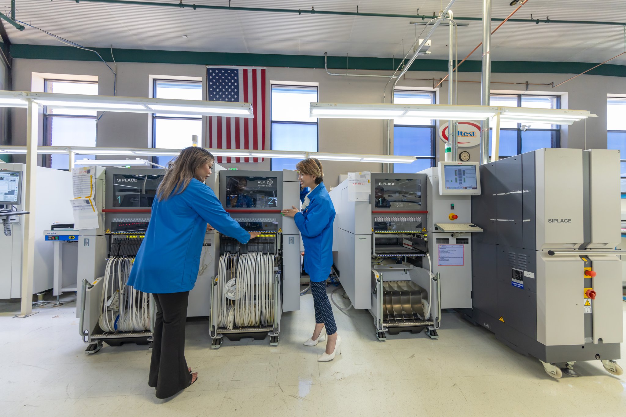
A two-line SMT production using ASM machines ensures high throughput, precision, and flexibility. Known for speed, reliability, and advanced features like intelligent placement and Industry 4.0 integration, ASM machines boost productivity while maintaining top-quality control.
Vapor Phase Vacuum Reflow is one of the most reliable SMT soldering processes, offering uniform heat transfer, oxidation-free soldering, and ultra-low voiding performance for BGA, QFN, LED, and high-reliability electronics.
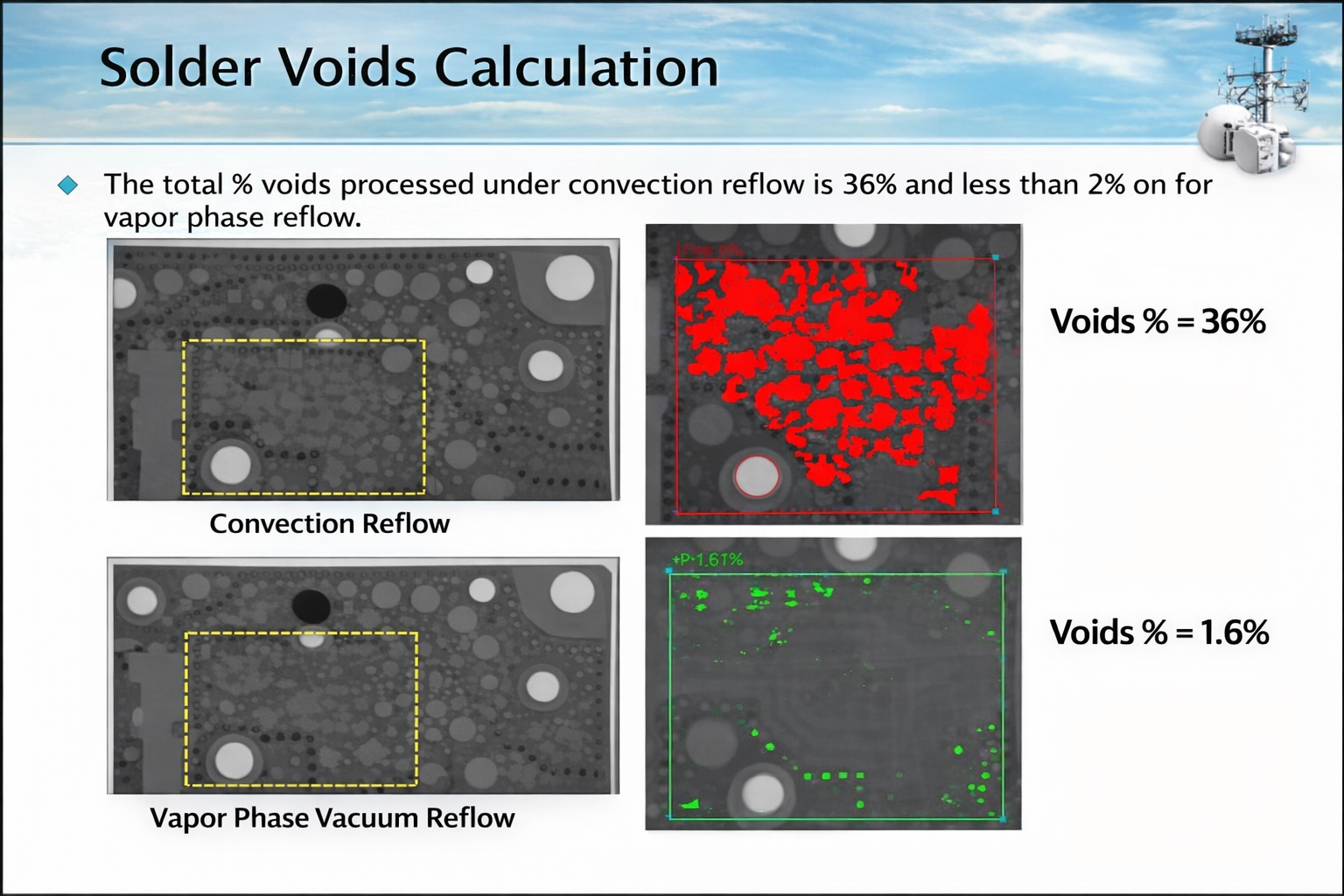
Multi Vacuum Process: With the innovative Multi Vacuum process, an assembly can be sequentially processed with multiple individually adjustable vacuum treatments.
Clean Vacuum Technology: With this patented process the vacuum process is performed outside the hot vapor zone.
< 1% Voids: Ultra-low void soldering for high-performance LED and thermal-critical assemblies.
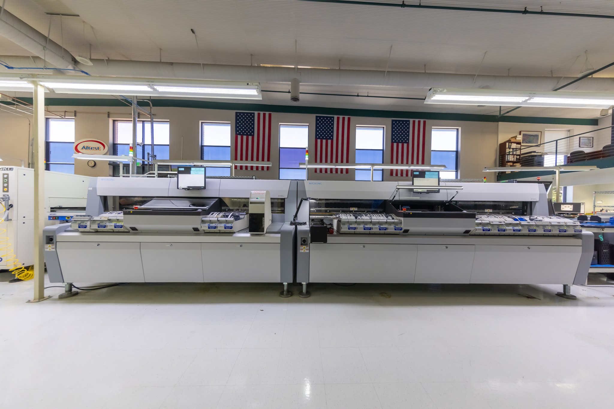
Our fully automated SMT assembly process supports a wide range of PCB technologies, including single-sided, double-sided, multilayer, HDI, rigid-flex, RF, and high-speed circuit boards. We assemble 01005 passive components, fine-pitch QFPs, BGAs, CSPs, LGAs, QFNs, PoP devices, and high-pin-count ICs with micron-level placement accuracy. Using intelligent component verification, automated optical alignment, and precision process control, we achieve consistent assembly quality while minimizing defects and maximizing production efficiency.
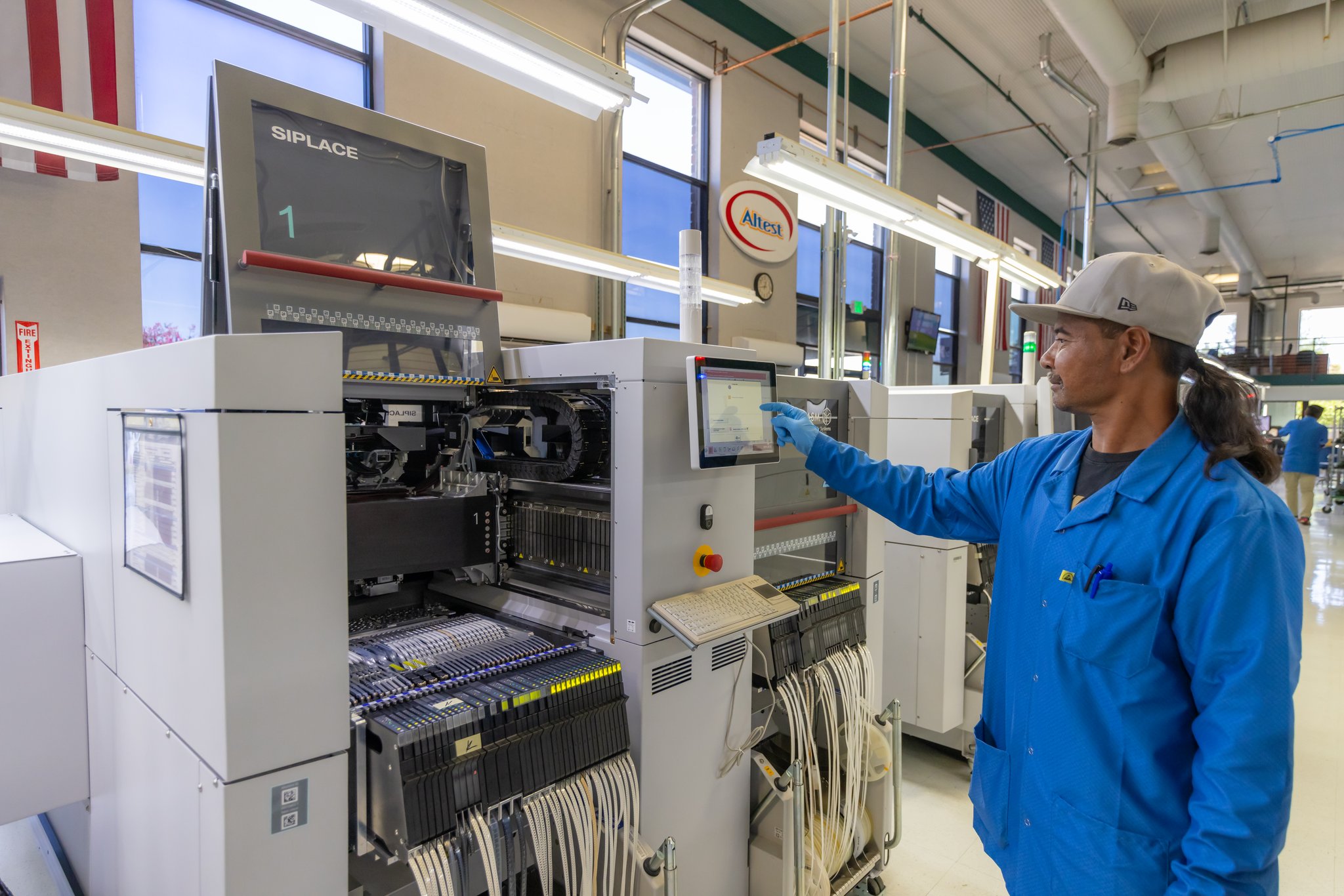
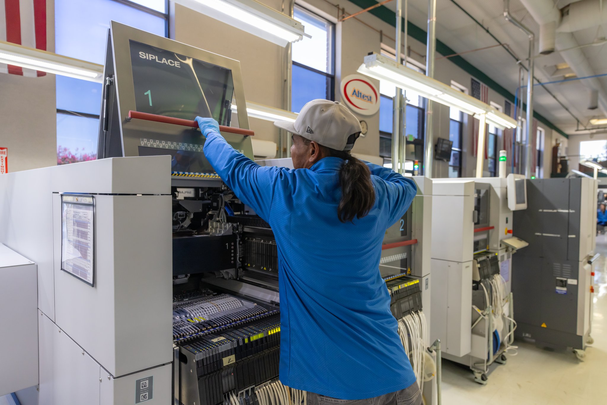
With decades of experience in Electronics Manufacturing Services (EMS), Altest Corporation is a trusted manufacturing partner for OEMs across aerospace, defense, medical devices, automotive, industrial automation, telecommunications, robotics, semiconductor, and consumer electronics. From component sourcing and PCB fabrication to SMT assembly, testing, box build integration, and final system assembly, we provide complete turnkey manufacturing solutions that reduce supply chain complexity, accelerate time-to-market, and deliver exceptional product quality.
Find answers to common questions about our automated pick-and-place capabilities, reflow soldering, component placement limits, and lead-free profiles.
SMT Assembly is the highly automated process of mounting electronic components directly onto the surface pads of a printed circuit board (PCB). It utilizes robotic pick-and-place machines to position parts onto wet solder paste, which is then melted in a reflow oven to create permanent electrical and mechanical connections.
SMT mounts components flat on the surface of the board, allowing for microscopic part sizes, higher routing density, and automated high-speed placement. Through-hole technology (THT) requires drilling holes completely through the PCB to insert component wire leads, which are then soldered on the bottom. THT is mostly reserved for heavy, bulky, or high-mechanical-stress components like large connectors.
Our state-of-the-art SMT lines are equipped with advanced optical alignment systems capable of placing ultra-miniature passive components down to the 01005 metric size. We can also routinely handle fine-pitch micro-BGAs and Chip Scale Packages (CSP) with pad spacing as tight as 0.3mm.
Our pick-and-place robots use flying-vision cameras to photograph both the board's fiducial markers and the component itself in mid-air. The machine's algorithm instantly calculates any required X, Y, and Theta (rotational) offsets before the nozzle gently sets the part down with sub-micron precision.
Reflow soldering involves passing the populated board through a multi-zone convection oven. We program a specific "thermal profile" for every unique board. This profile dictates the exact temperature ramp-up, soak time, peak reflow heat, and cooling rate to ensure the solder melts perfectly without thermally shocking or destroying sensitive silicon components.
Yes. We run strictly segregated lead-free (RoHS-compliant, like SAC305) and leaded (SnPb) assembly processes. While commercial electronics demand lead-free processing, our aerospace, military, and critical medical customers often require traditional leaded solder to completely mitigate the risk of tin-whisker growth.
Every board goes through 100% inline 3D Automated Optical Inspection (AOI) to verify component presence, correct polarity, and optimal solder fillet volume. For hidden solder joints located underneath components (like BGAs, QFNs, or LGA packages), we utilize High-Resolution 3D X-Ray (AXI) inspection to check for shorts, opens, and unacceptable voiding.
Absolutely. Double-sided SMT assembly is standard for dense designs. We first print, populate, and reflow the top side. We then flip the board and repeat the process on the bottom. We carefully engineer the thermal profiles (and utilize specialized SMT adhesives if necessary) to ensure heavy components on the bottom side do not drop off during the second reflow cycle.
If AOI or X-Ray flags a defect, the board is diverted to our IPC-7711/7721 certified rework stations. Highly trained technicians use specialized, localized thermal heating to safely remove the bad component, clean the pads, and place a new component without thermally stressing the rest of the finished board.
Yes. We specialize in fast-turn NPI and prototyping. We offer scalable solutions, meaning we can assemble your first 5-piece proof-of-concept run using the exact same robotic lines and quality controls that will eventually be used for your 10,000-piece high-volume production run.
Partner with Altest Corporation for your next high-reliability PCB fabrication and turnkey SMT assembly project. Our engineering team is ready to review your gerber files and provide a detailed, competitive estimate.

