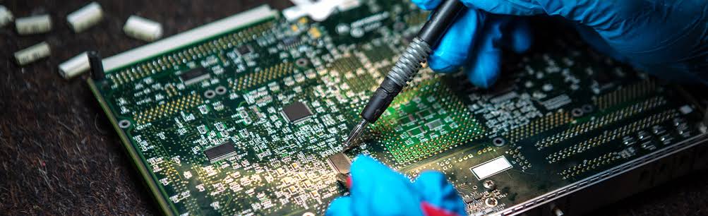
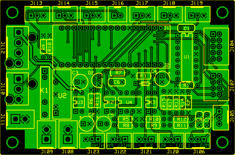
Our PCB Reverse Engineering Services help businesses recover complete design data from existing printed circuit boards, electronic assemblies, and obsolete products. Whether the original design files are missing or outdated, our experienced engineers recreate accurate schematics, PCB layouts, Gerber files, Bills of Materials (BOM), and manufacturing documentation. Using advanced inspection and analysis techniques, we transform physical boards into production-ready digital designs, enabling redesign, repair, product upgrades, and long-term manufacturing support. Our reverse engineering process minimizes downtime while preserving the functionality and performance of your electronic systems.
Recover lost design files, recreate accurate schematics, and modernize legacy electronic products with our professional PCB reverse engineering services.
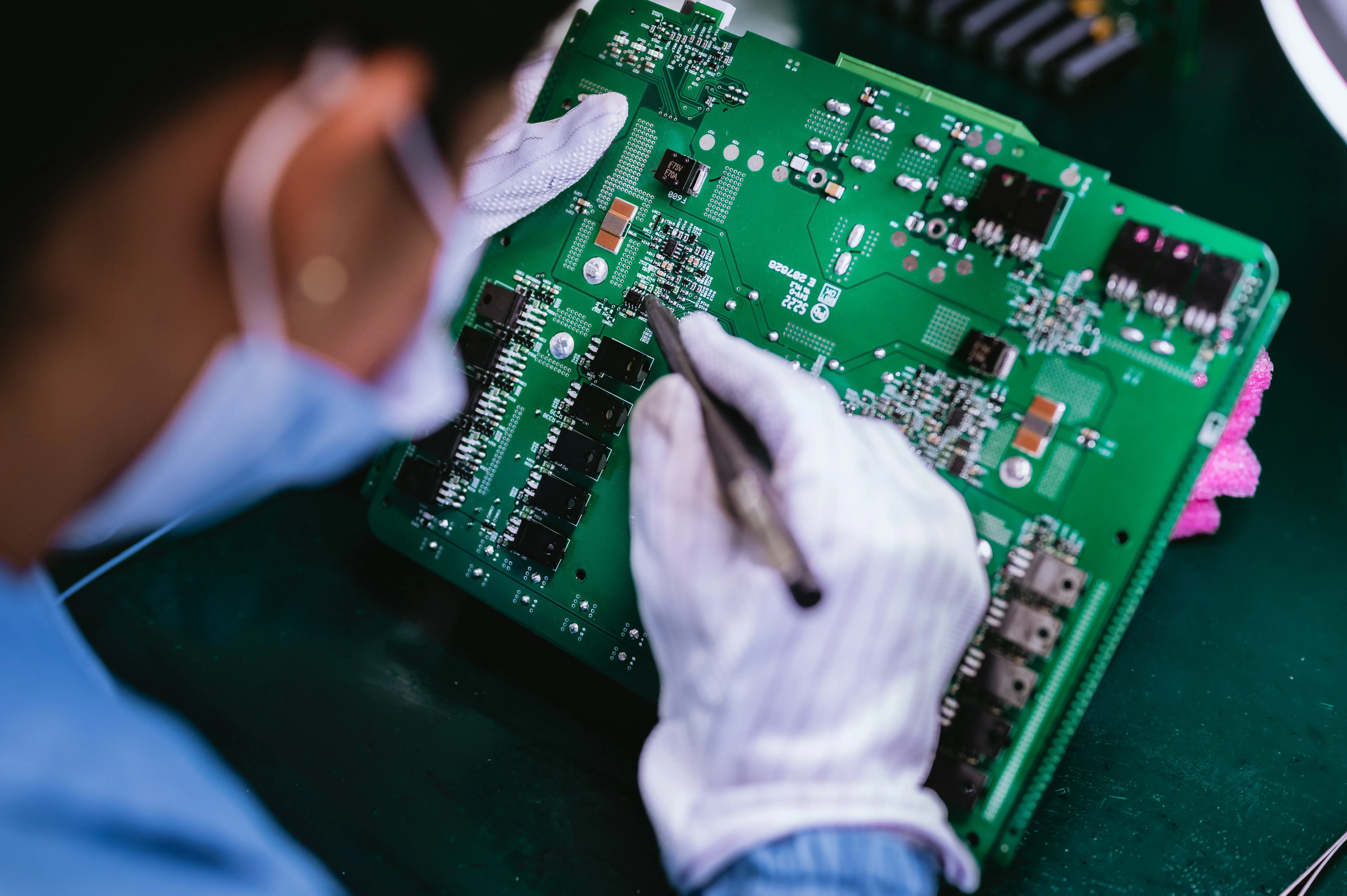
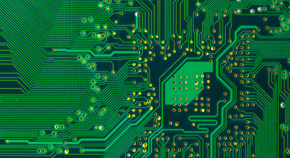
Every reverse engineering project begins with a detailed examination of the PCB structure, components, signal routing, layer stack-up, and electrical connectivity. We carefully identify obsolete or end-of-life components, verify circuit functionality, and reconstruct complete design documentation using industry-leading CAD tools. From single-layer boards to complex multilayer, HDI, RF, and high-speed PCBs, our engineers ensure the recreated design accurately reflects the original product while incorporating improvements for manufacturability, reliability, and future scalability.
Reverse engineering is an effective solution for extending the life of legacy electronics, replacing discontinued components, and preparing products for modern manufacturing. Our engineering team can optimize existing designs through Design for Manufacturing (DFM) and Design for Test (DFT) reviews, ensuring improved production efficiency and product reliability. Whether you need to duplicate an existing PCB, modernize aging hardware, support field repairs, or develop a next-generation version of your product, we deliver complete engineering solutions tailored to your business requirements.
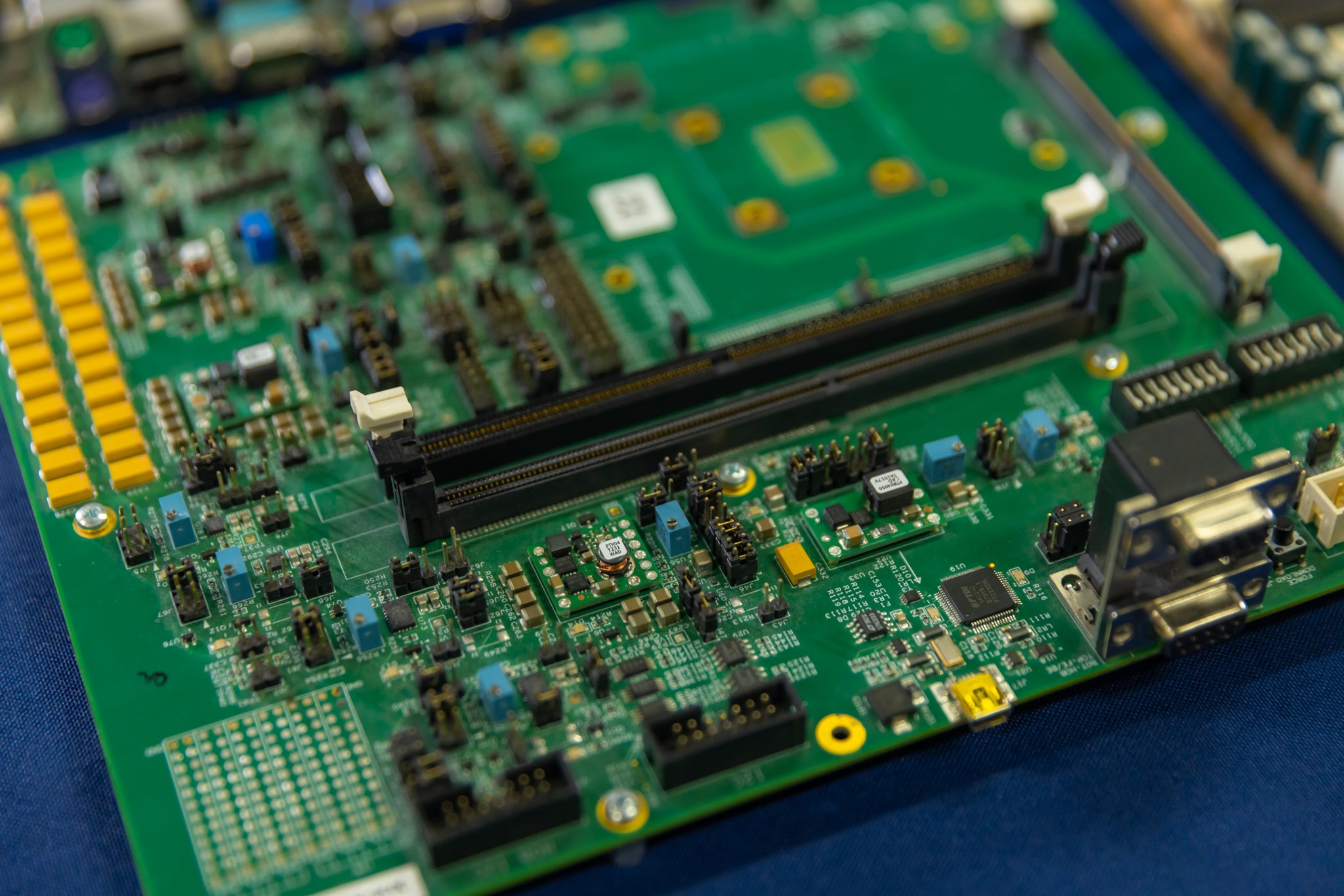
With decades of experience in PCB design, PCB fabrication, PCB assembly, and electronic engineering, Altest Corporation provides reliable reverse engineering services for industries including aerospace, defense, medical, industrial automation, telecommunications, automotive, and consumer electronics. Our end-to-end capabilities—from schematic capture and PCB layout to prototyping, testing, and full-scale production—allow us to deliver accurate, manufacturing-ready designs with faster turnaround times. By combining advanced engineering expertise with strict quality standards, we help customers reduce development costs, protect valuable intellectual assets, and confidently bring legacy electronic products back into production.
Find answers to common questions about our bare board extraction, legacy product recreation, and destructive/non-destructive scanning processes.
PCB reverse engineering is the process of analyzing a physical printed circuit board to extract its design data. When original CAD files, schematics, or BOMs (Bill of Materials) are lost or corrupted, we deconstruct the physical board to digitally recreate the manufacturing files required to build it again.
For simple 1- or 2-layer boards, non-destructive optical scanning is usually sufficient. However, for complex multi-layer boards, the process is destructive. We must carefully sand or mill down the board layer by layer to photograph and map the internal copper traces and blind/buried vias.
Yes. Utilizing advanced 3D tomographic scanning, high-resolution X-ray, and precision CNC delayering, our engineering team can successfully extract the netlist and layout geometry of high-density interconnect (HDI) boards with complex multi-layer stackups.
If chips have had their part numbers sanded off to hide intellectual property, or if they are decades old, we use a combination of XRF elemental analysis, chemical decapsulation, curve tracer pin testing, and cross-referencing against our massive legacy component database to identify the correct part or find a drop-in replacement.
Yes, the form, fit, and electrical function will match the original legacy hardware perfectly. However, during the process, we often implement modern DFM (Design for Manufacturing) upgrades and replace obsolete through-hole parts with modern SMT equivalents to improve the board's longevity and reduce future manufacturing costs.
If the microcontroller, FPGA, or memory chip is not locked or encrypted with security bits, we can read and extract the hex/bin code. If the chip is locked, extracting the firmware requires specialized silicon-level invasive techniques which may be discussed on a case-by-case basis.
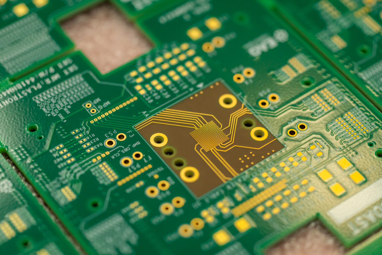
Upon project completion, you will receive a comprehensive data package. This includes native CAD files (such as Altium Designer), a newly generated logical schematic, a verified Bill of Materials (BOM), Gerber/ODB++ fabrication files, and pick-and-place centroid data for assembly.
Timelines are highly dependent on the complexity of the board, the layer count, and the density of the component population. A simple legacy 2-layer board might take 1 to 2 weeks, while a dense 12-layer HDI board could take 4 to 8 weeks to properly extract and verify.
Generally, yes. Reverse engineering is legally recognized as a valid method for interoperability, maintaining legacy systems, and independent research. However, we strictly adhere to IP laws and will not duplicate patented silicon structures or proprietary encrypted software code intended to counterfeit protected intellectual property.
Yes. Once the reverse engineering contract is complete and the final deliverables are handed over, Altest Corporation transfers full ownership of the newly generated CAD files, schematics, and netlist data directly to your company.
Partner with Altest Corporation for your next high-reliability PCB fabrication and turnkey SMT assembly project. Our engineering team is ready to review your gerber files and provide a detailed, competitive estimate.

