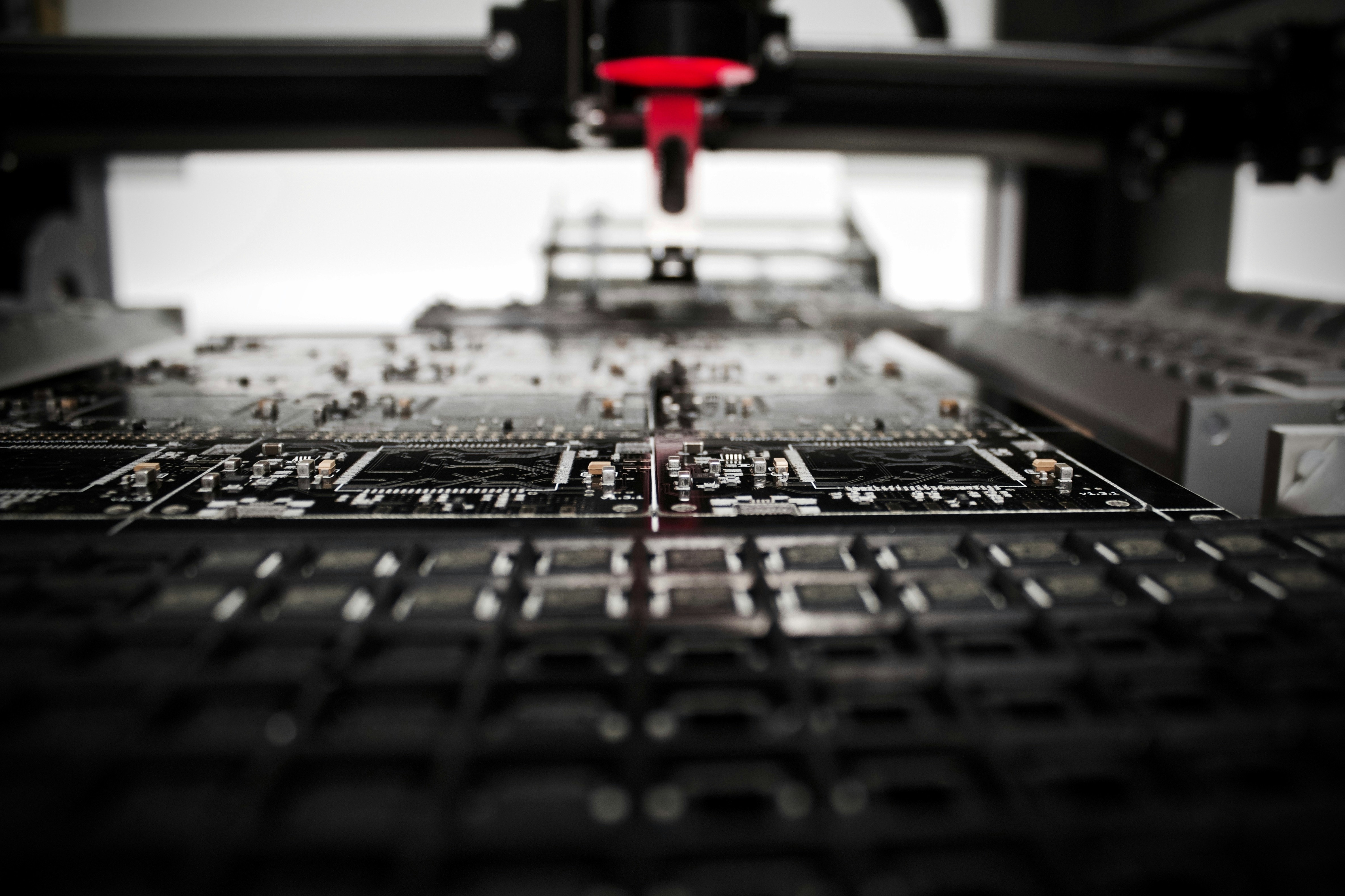
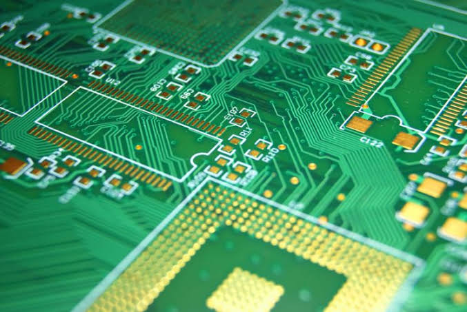
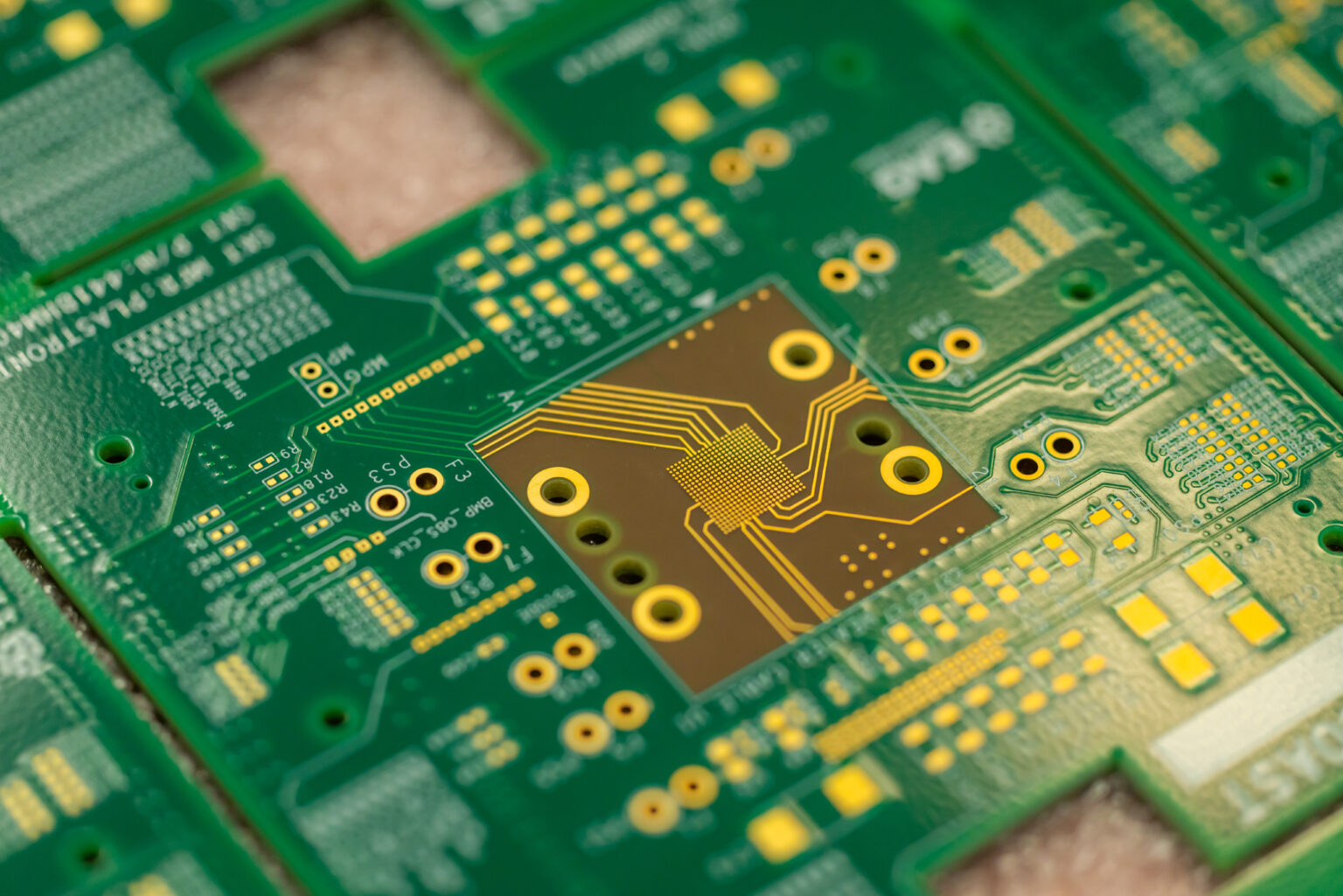
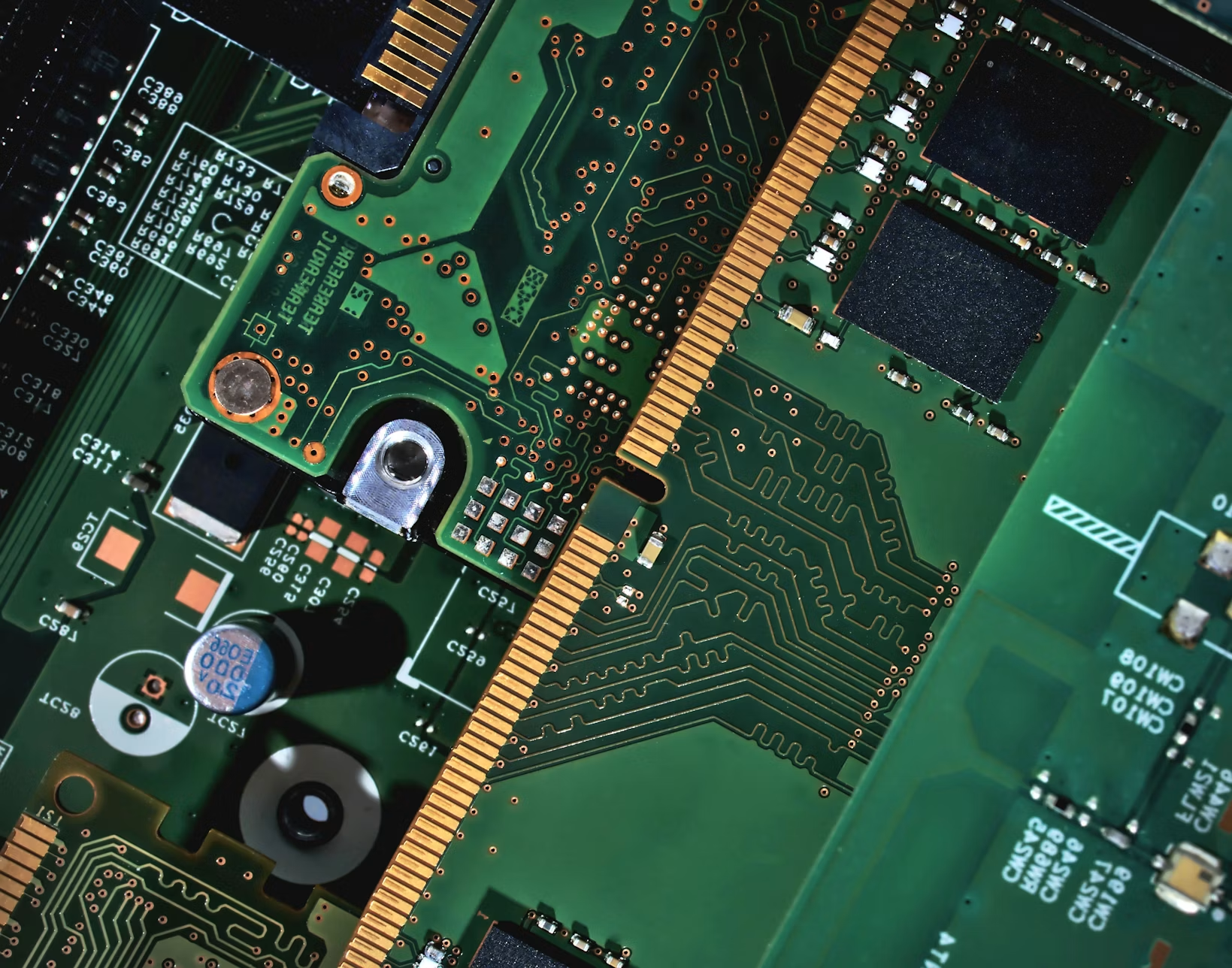
Our PCB Fabrication Services deliver high-quality, precision-manufactured printed circuit boards for prototypes, low-volume production, and high-volume manufacturing. At Altest Corporation, we combine advanced manufacturing technologies, strict quality control, and IPC-compliant processes to produce reliable PCBs that meet the performance demands of industries such as aerospace, medical, automotive, telecommunications, industrial automation, and consumer electronics. From standard two-layer boards to complex HDI, multilayer, RF, and rigid-flex PCBs, we ensure exceptional quality, fast turnaround times, and consistent manufacturing excellence.
From rapid prototypes to high-volume production, our PCB fabrication services deliver precision, reliability, and exceptional quality for every project.
.jpg)
We manufacture a wide range of PCB technologies using state-of-the-art equipment and industry-leading fabrication processes. Our capabilities include single-sided, double-sided, multilayer, HDI, flexible, rigid-flex, RF & microwave, aluminum, ceramic, heavy copper, and high-frequency PCBs. Every board is manufactured with precise trace widths, controlled impedance, high-quality surface finishes, and rigorous inspection standards to ensure superior electrical performance and long-term reliability. Our engineering team also performs comprehensive Design for Manufacturing (DFM) reviews to identify potential production issues before fabrication begins.
Quality is integrated into every stage of our PCB fabrication process. We use premium-grade materials, automated optical inspection (AOI), electrical testing, X-ray inspection, flying probe testing, and IPC-certified manufacturing practices to verify every PCB before delivery. Whether you require a rapid prototype for product validation or full-scale production for commercial applications, we provide flexible manufacturing solutions that reduce lead times, improve yields, and ensure consistent product performance. Our end-to-end support also includes PCB assembly, component sourcing, testing, and box build services for a complete electronics manufacturing solution.
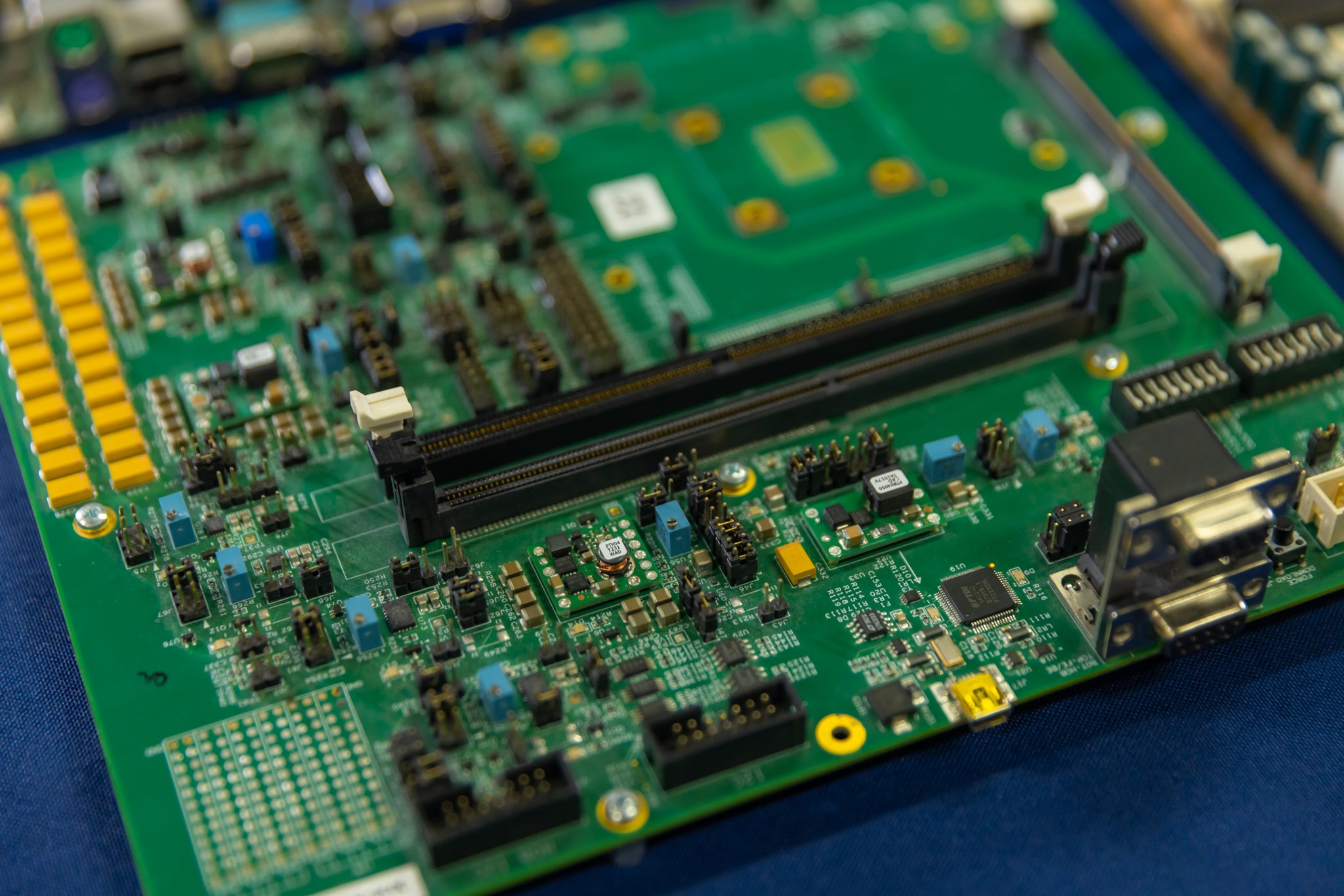
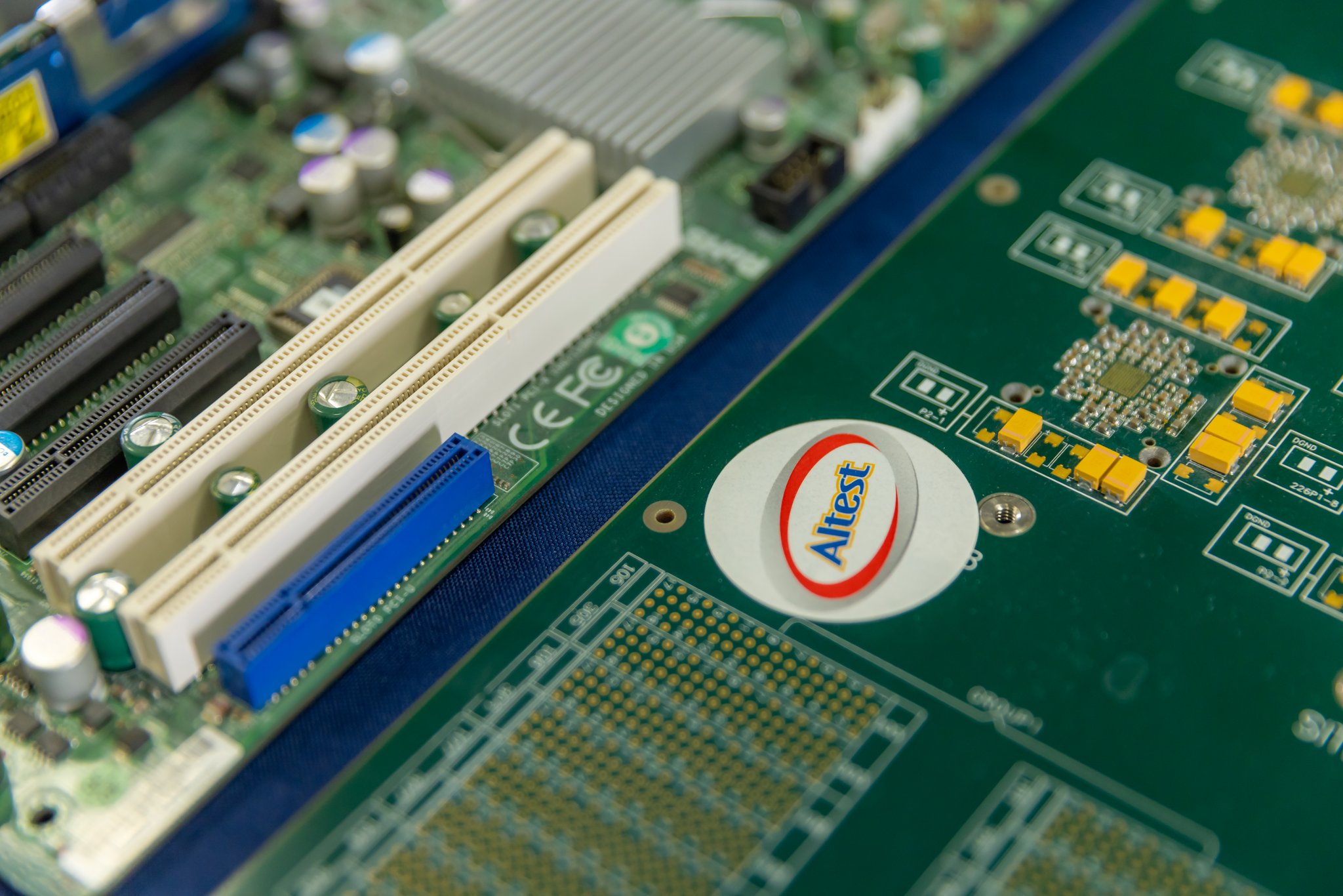
With decades of experience in PCB manufacturing and electronic engineering, Altest Corporation is a trusted partner for businesses seeking reliable, high-performance circuit boards. Our experienced engineers, advanced manufacturing facilities, and commitment to quality enable us to deliver cost-effective PCB fabrication services tailored to your exact specifications. By combining engineering expertise, fast production capabilities, strict quality assurance, and exceptional customer support, we help customers accelerate product development, reduce manufacturing risks, and bring innovative electronic products to market with confidence.
Find answers to common questions about our bare board manufacturing, material options, layer counts, and high-density interconnect (HDI) capabilities.
PCB fabrication is the process of transforming a digital circuit board design (Gerber files) into a physical bare board. It involves laminating copper to substrate materials, etching traces, drilling vias, and applying solder mask and silkscreen to create the foundation for electronic components.
We utilize a wide variety of high-quality materials depending on your application's requirements. This includes standard FR-4 (High-Tg), Rogers or Nelco for high-frequency/RF designs, polyimide for flex circuits, and aluminum/copper core materials for advanced thermal management.
Altest Corporation is fully equipped to manufacture highly complex, high-density multi-layer boards up to 40 layers. Our advanced presses ensure strict layer-to-layer registration, precise impedance control, and structural integrity for critical applications.
Yes, we specialize in advanced HDI PCB fabrication. Our Silicon Valley facility supports laser-drilled blind and buried vias, stacked and staggered micro-vias, and ultra-fine trace/space resolutions to easily accommodate complex, high-pin-count components like fine-pitch BGAs.
We offer a comprehensive range of RoHS-compliant and standard surface finishes to protect the copper circuitry and provide a solderable surface. Options include Electroless Nickel Immersion Gold (ENIG), Hot Air Solder Leveling (HASL) Lead-Free, OSP, Hard Gold, Immersion Silver, and Immersion Tin.
Turnaround times are scalable based on board complexity and order quantity. For standard quick-turn prototypes, we can deliver bare boards in as little as 24 to 48 hours. Standard volume production runs typically range from 5 to 10 business days.
Absolutely. 100% of our fabricated bare boards undergo rigorous electrical testing before they are shipped or moved to assembly. We primarily utilize automated Flying Probe or Bed-of-Nails testing to guarantee there are no open circuits or hidden shorts.
To provide an accurate quote and begin the manufacturing process, we require your complete Gerber data (RS-274X) or ODB++ files, an NC Drill file, a fabrication drawing detailing board dimensions and stackup, and an IPC-D-356 netlist.
Yes. Our primary quick-turn fabrication and assembly operations are located entirely within the United States at our facility in San Jose, California. This ensures the highest level of quality control, intellectual property protection, and strict ITAR compliance.
Yes, we strictly adhere to environmental and safety standards. We offer fully RoHS-compliant manufacturing processes utilizing lead-free materials. Additionally, our boards are manufactured to meet or exceed IPC Class II and Class III standards, and carry necessary UL certifications.
Partner with Altest Corporation for your next high-reliability PCB fabrication and turnkey SMT assembly project. Our engineering team is ready to review your gerber files and provide a detailed, competitive estimate.

