Speed:AOI is much faster than manual inspection, allowing for real-time feedback and quicker detection of defects, which is critical in high-volume manufacturing environments.
Consistency:The automated nature of AOI ensures that inspections are consistent across the entire production run, reducing human error and variability.
High Accuracy:AOI systems can detect minute defects with incredible accuracy, including very small soldering issues, surface imperfections, or minor misalignments that would be hard for the human eye to detect.
Cost-Effective:While AOI systems may require an initial investment in equipment, they can significantly reduce labor costs associated with manual inspection, and they can operate 24/7 without fatigue.
Automated Optical Inspection is one of the most effective methods for ensuring manufacturing excellence in modern electronics. By combining high-resolution imaging, intelligent defect recognition, and real-time process monitoring.
.jpg)
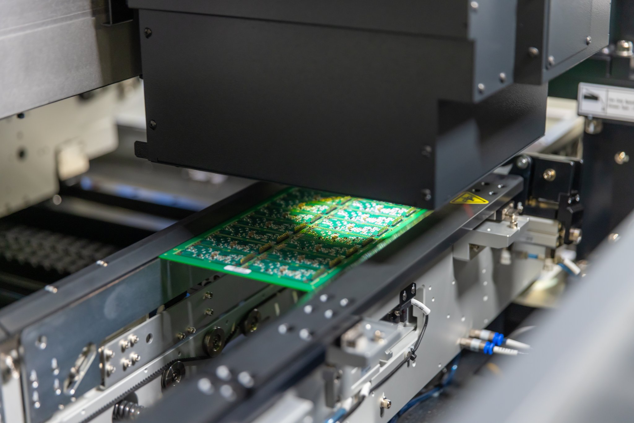
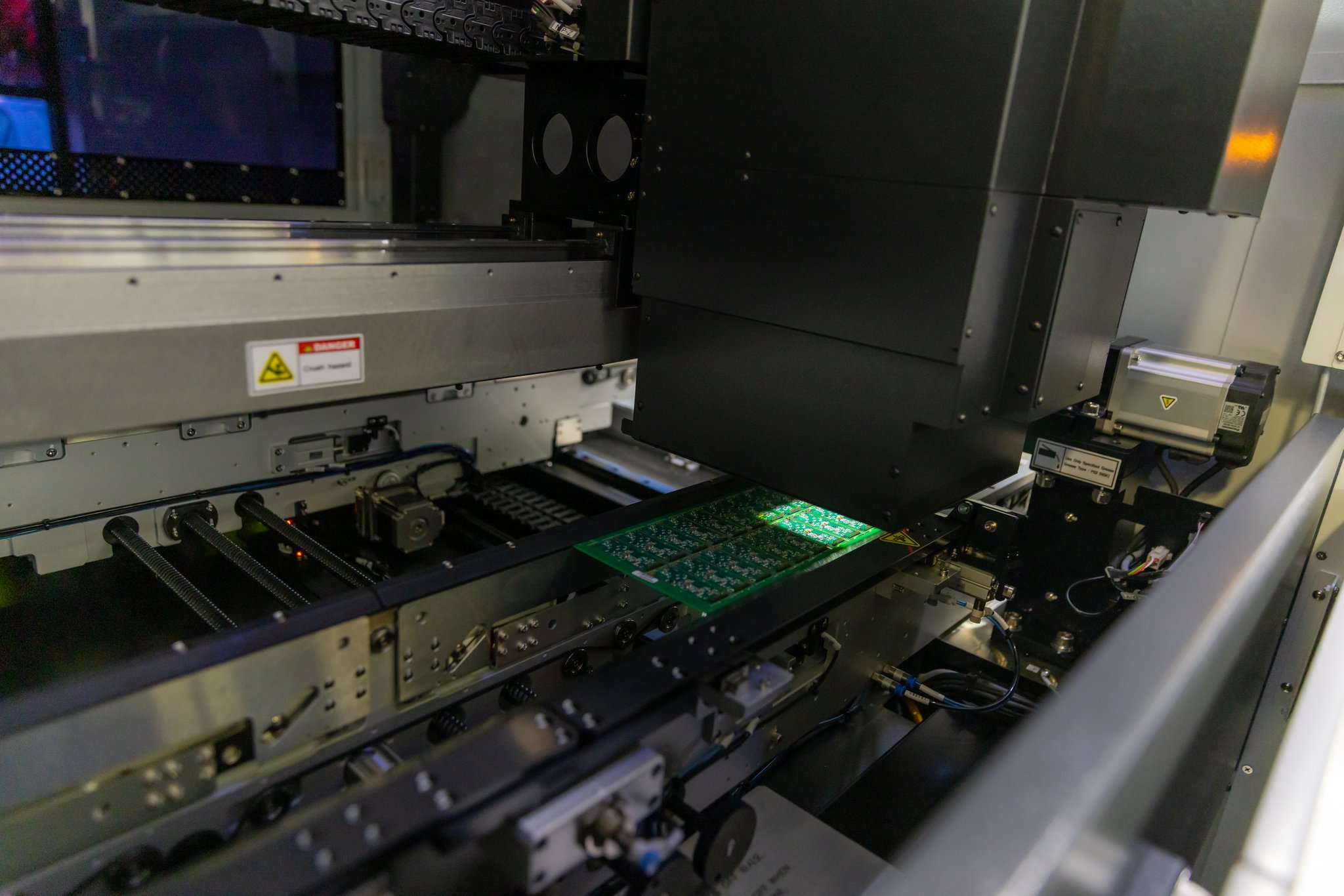
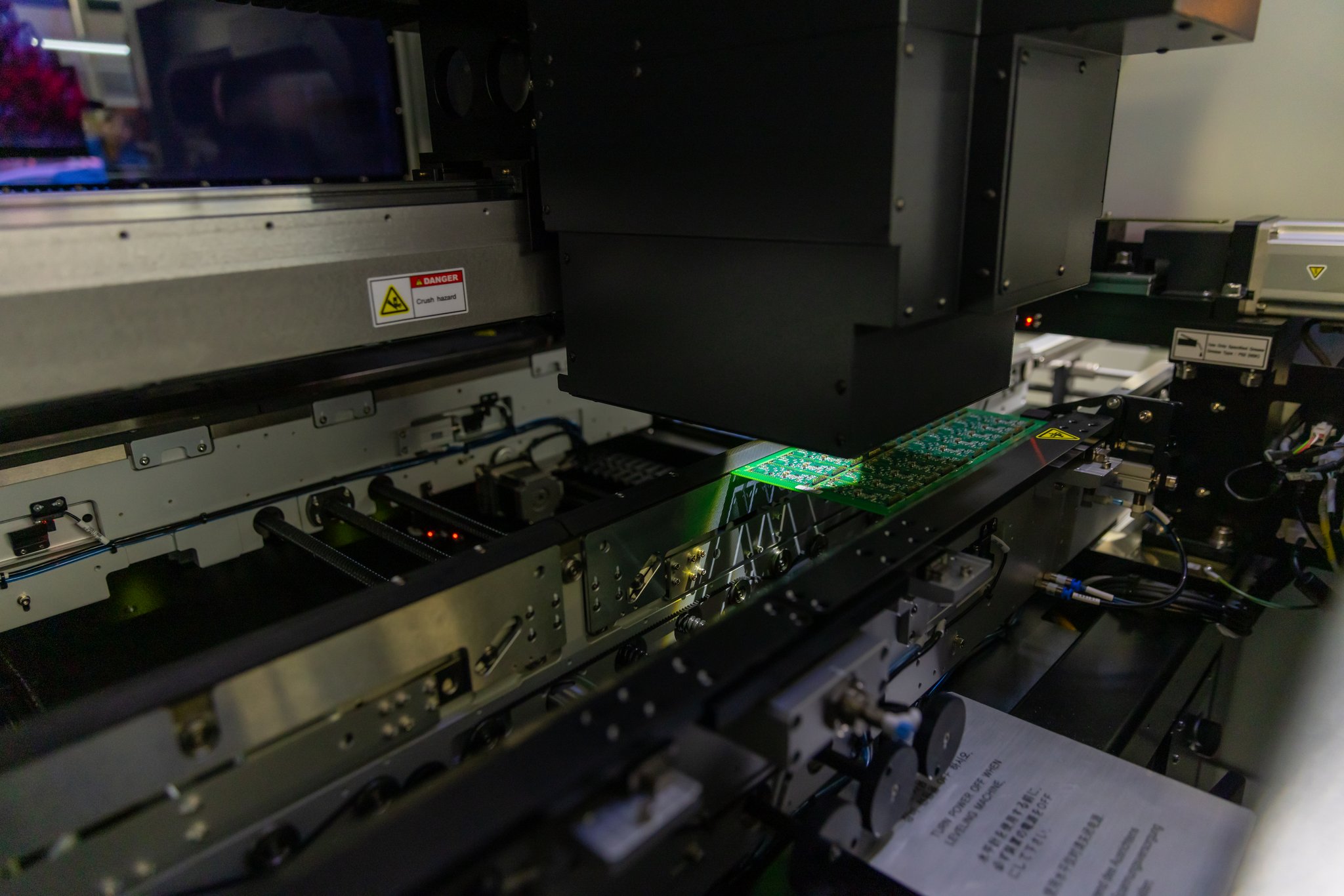
Our AOI systems inspect every printed circuit board against CAD data and Golden Board references to identify even the smallest manufacturing deviations. The inspection process accurately detects missing components, incorrect component placement, polarity errors, solder bridges, insufficient solder, excess solder, lifted leads, tombstoning, skewed components, open solder joints, damaged components, and PCB surface defects. This automated inspection capability ensures consistent product quality across prototype, low-volume, and high-volume production while maintaining micron-level inspection accuracy.
AOI plays a vital role in our closed-loop manufacturing process by providing real-time production feedback that enables continuous process optimization. Inspection data is analyzed to identify trends, improve stencil printing, optimize pick-and-place accuracy, and reduce process variation. Our AOI workflow is fully integrated with Solder Paste Inspection (SPI), X-Ray Inspection (AXI), In-Circuit Testing (ICT), Flying Probe Testing, Functional Testing, and Statistical Process Control (SPC) to deliver comprehensive quality assurance throughout the SMT manufacturing process. Every inspection follows IPC quality standards to ensure repeatable, defect-free production.
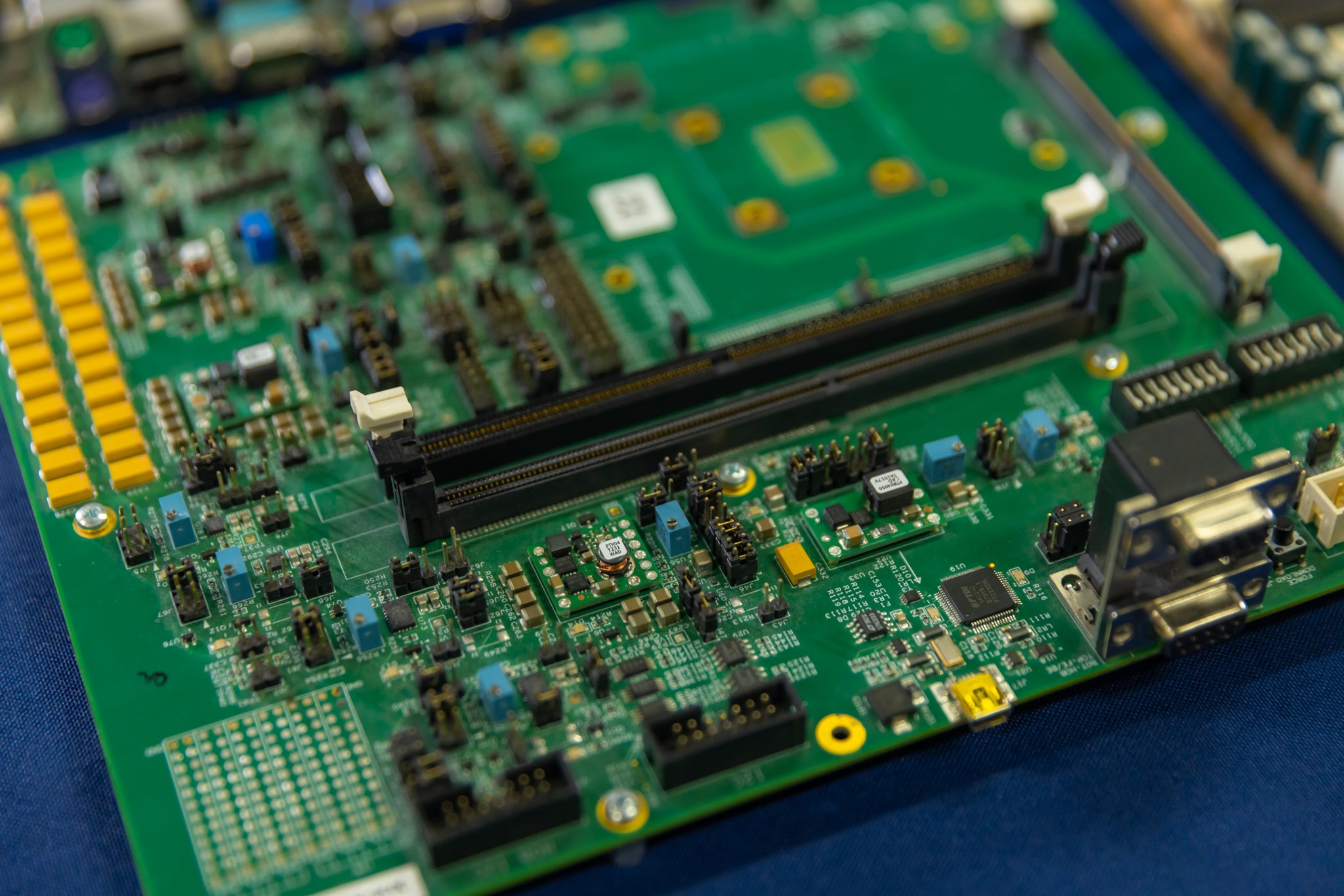
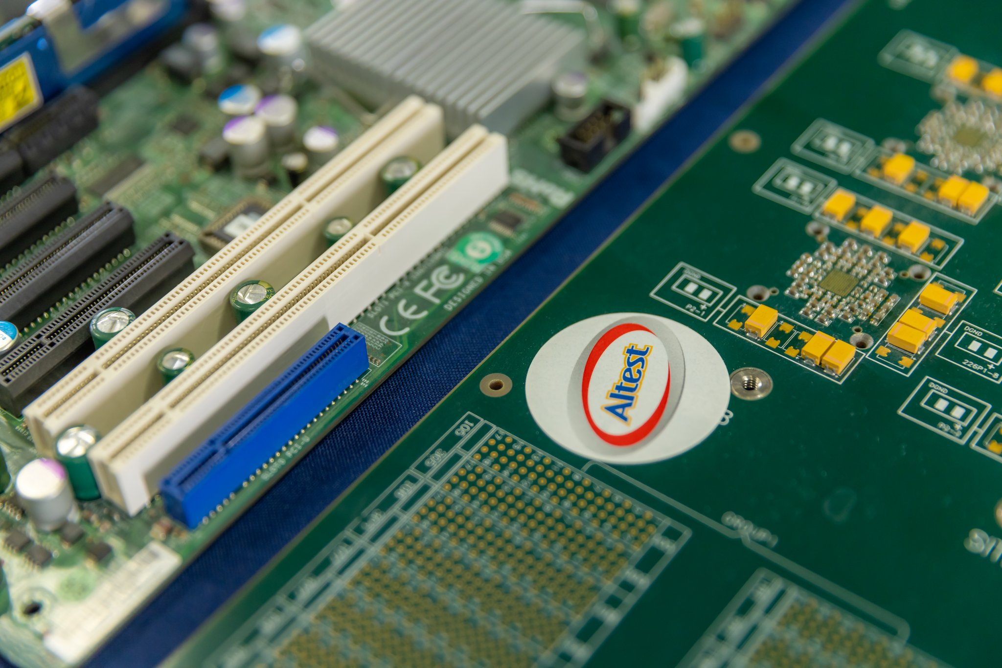
With decades of experience in PCB manufacturing and Electronics Manufacturing Services (EMS), Altest Corporation utilizes the latest 2D and 3D AOI technology to verify every PCB assembly with exceptional speed and precision. Our experienced quality engineers, automated inspection systems, and rigorous IPC-compliant processes enable us to deliver consistently high-quality assemblies for industries including aerospace, defense, medical devices, automotive, telecommunications, industrial automation, semiconductor, and consumer electronics.
Find answers to common questions about 3D AOI technology, defect detection, inline inspection processes, and quality assurance standards.
Automated Optical Inspection (AOI) is a highly accurate, machine-vision-based quality control process. It utilizes high-resolution cameras and specialized lighting arrays to autonomously scan printed circuit board assemblies (PCBAs) for catastrophic failure defects (like missing parts) and quality defects (like skewed components or poor solder joints).
As modern electronic components shrink to microscopic sizes (like 01005 metric discretes) and board densities increase, the human eye simply cannot reliably inspect thousands of solder joints per minute without suffering from severe fatigue. AOI provides 100% consistent, objective, and lightning-fast inspection that catches defects humans would inevitably miss.
AOI systems are programmed to detect a wide array of SMT defects. These include component presence/absence, X/Y positional skew, rotational misalignment, incorrect polarity/orientation, tombstoning, solder bridges (shorts), insufficient solder fillets (opens), and lifted component leads.
2D AOI uses top-down cameras to check component presence and X/Y alignment based on color and contrast. 3D AOI uses lasers and structured light to create a full topographical map of the board. 3D AOI is vastly superior because it can accurately measure the Z-height of a component (detecting lifted leads) and calculate the true volumetric mass of a solder fillet. We utilize inline 3D AOI exclusively for our SMT lines.
AOI can be placed at multiple stages. Most commonly, it is used "Post-Reflow" as a final quality gate before the board moves to the next department. However, for critical high-volume runs, we also utilize "Pre-Reflow" AOI immediately after pick-and-place. Catching a misaligned component before the solder is baked makes rework incredibly fast and inexpensive.
No. AOI requires a direct line-of-sight to inspect a solder joint. For components with bottom-terminated pads like Ball Grid Arrays (BGAs), Quad Flat No-leads (QFNs), or Land Grid Arrays (LGAs), we must use our 3D X-Ray (AXI) inspection systems to look "through" the silicon packaging to verify the joints.
Not at all. Modern inline 3D AOI machines feature high-speed linear motors, massive field-of-view cameras, and parallel processing algorithms. They can scan densely populated boards in a matter of seconds, easily keeping pace with the fastest robotic pick-and-place machines without becoming a manufacturing bottleneck.
A false call (or false fail) occurs when the AOI machine flags a perfectly acceptable solder joint or component as a defect. This is usually caused by variations in board coloration or slight changes in component supplier packaging. Our engineers continuously fine-tune the AOI algorithms and lighting thresholds to minimize false calls and maximize throughput.
Yes. While primarily used for SMT, AOI can be configured to inspect Through-Hole Technology (THT) assemblies. It can scan the top of the board to verify component insertion and polarity, and it can scan the bottom of the board after wave soldering to verify proper hole fill, pin length, and the absence of solder bridging.
Yes. Our AOI systems are integrated directly into our Factory Information System via 2D barcodes or QR codes on the PCB. The machine saves a complete 3D topographical map and high-resolution images of every component for every board produced. This provides absolute defect traceability for aerospace, military, and medical (FDA) compliance.
Partner with Altest Corporation for your next high-reliability PCB fabrication and turnkey SMT assembly project. Our engineering team is ready to review your gerber files and provide a detailed, competitive estimate.

