

Flying Probe Testing Services: A Crucial Component in PCB Quality Assurance
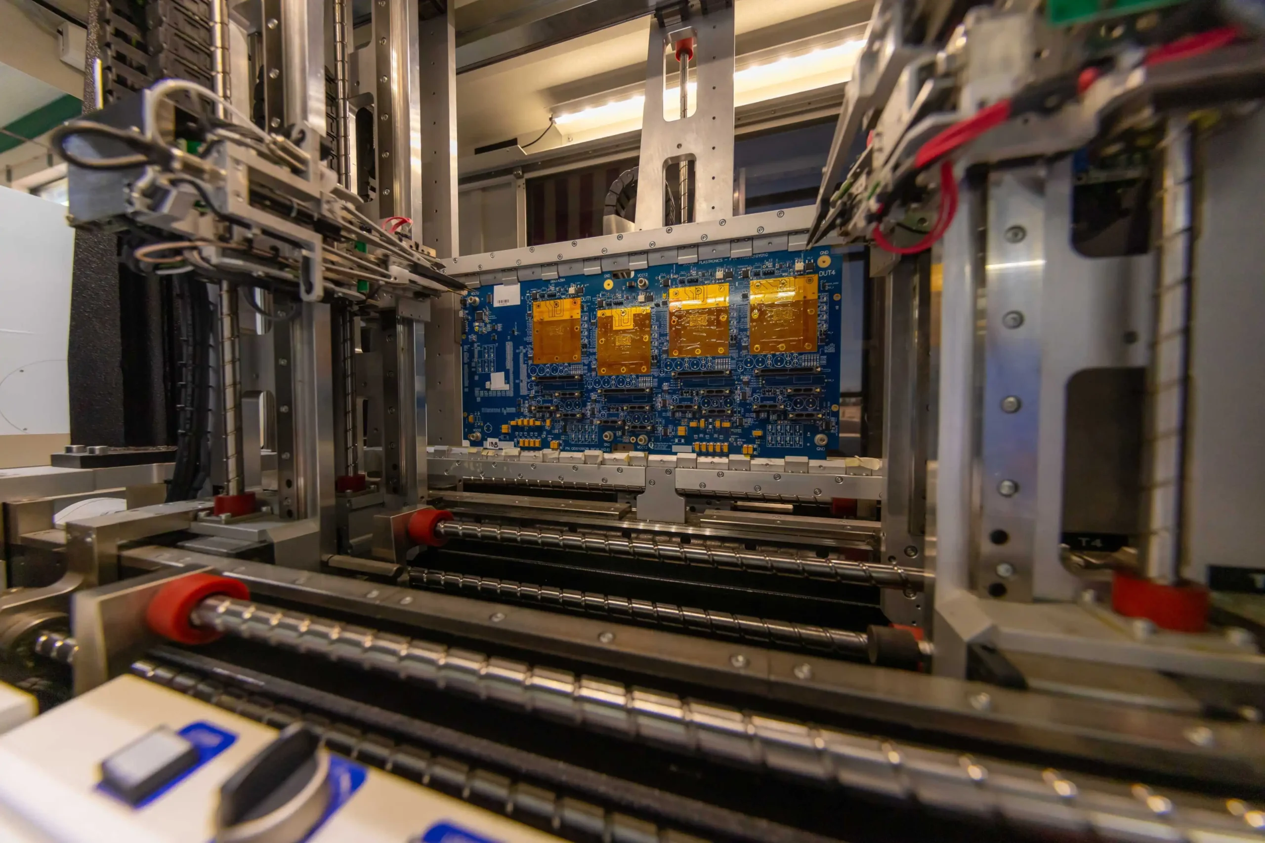
In today’s electronics manufacturing industry, where precision and reliability are paramount, Flying Probe Testing (FPT) has emerged as an invaluable tool for PCB quality assurance. Flying probe testing services provide flexible, high-accuracy testing of printed circuit boards (PCBs), allowing manufacturers to identify and correct potential faults in assembled boards before they reach consumers.
This article discusses the mechanics of flying probe testing, its benefits, and its role in modern electronics manufacturing.
What Is Flying Probe Testing?
Flying probe testing is a method of testing PCBs that employs moving probes to inspect each node (test point) on a board without requiring fixed test fixtures.
Unlike traditional In-Circuit Testing (ICT), which uses a bed-of-nails fixture to make connections, FPT uses a series of robotic arms or probes that “fly” across the PCB. These probes make contact with specific points on the board to test for:
- Electrical connectivity
- Component values
- Shorts
- Opens
- Other potential PCB defects
The lack of a fixed test fixture makes flying probe testing ideal for low- to medium-volume production runs, prototypes, and complex PCBs.
With its flexibility and high precision, flying probe testing is widely used in industries that prioritize quality, including:
- Automotive
- Aerospace
- Medical
- Telecommunications
- Consumer electronics
How Does Flying Probe Testing Work?
Flying probe testing involves several key steps to inspect and verify the electrical performance of a PCB.
1. Test Program Development
The FPT system is programmed to identify the specific locations on the PCB that need to be tested. It is loaded with the board’s layout data, including component locations and expected electrical characteristics.
2. Probing Process
Robotic probes move across the PCB at high speed, contacting each test point as programmed. The test probes can access densely packed boards and are often configured to reach both the top and bottom sides of a PCB.
3. Electrical Testing
The probes check for electrical continuity, resistance, capacitance, and other parameters. Some systems can also test diode polarity, transistor orientation, and other component-specific properties.
4. Data Analysis
Once testing is complete, the FPT system generates a report identifying any faults detected on the board. Engineers can then analyze the data to diagnose and rectify issues before the PCB moves on to the next stage of production.
Key Benefits of Flying Probe Testing
1. No Need for a Dedicated Test Fixture
Unlike ICT, flying probe testing requires no custom test fixture. This reduces setup costs and lead times, especially for low-volume or prototype production runs.
The flying probes can also be reprogrammed quickly, allowing manufacturers to make efficient changes between different PCB designs.
2. Flexibility for Various PCB Designs
Flying probe systems can handle a wide range of PCB layouts and complexities, from single-sided boards to multi-layer, densely packed designs.
This flexibility is particularly valuable for manufacturers working with prototypes or frequently changing product lines.
3. Cost-Effective for Low- to Medium-Volume Production
For small production runs, the cost of creating a dedicated test fixture for ICT may be prohibitive.
Flying probe testing provides a cost-effective solution by eliminating fixture costs and allowing manufacturers to test smaller production batches efficiently.
4. High Precision and Accuracy
Advanced flying probe testers are capable of measuring very fine pitches and testing complex configurations.
With precise robotic movement and intelligent programming, these systems can identify subtle defects that may be missed by other testing methods.
5. Rapid Turnaround for Prototypes
During the prototype stage, PCB designs may undergo frequent changes. Flying probe testing provides rapid adaptability, allowing manufacturers to quickly adjust test programs for new PCB revisions.
This helps expedite the testing and development cycle.
Applications of Flying Probe Testing
1. Prototype Testing
For electronics companies developing new products, flying probe testing is ideal for testing prototypes quickly and effectively.
As new designs are introduced, FPT can adapt to each iteration without requiring a new fixture. This allows manufacturers to identify and resolve issues early in the development cycle.
2. Small Batch Testing
Flying probe testing is suitable for manufacturers producing low to medium quantities, such as specialized or niche electronics.
These manufacturers benefit from the lower cost and flexibility of FPT because it eliminates the need to invest in fixed test fixtures.
3. High-Mix, Low-Volume Manufacturing
For production environments that handle various PCB designs, flying probe testing provides the ability to switch quickly between jobs.
This makes FPT ideal for contract manufacturers serving multiple customers with different PCB designs.
4. Quality Assurance for Complex PCBs
Advanced, high-density PCBs with multiple layers, intricate vias, and fine-pitch components require precise testing.
Flying probe testing provides the accuracy needed to test these intricate designs, helping ensure reliability and performance in demanding applications such as aerospace and medical devices.
Advances in Flying Probe Testing Technology
1. Enhanced Testing Speed
Modern flying probe systems are designed to operate at higher speeds, with some models using multiple probes per side.
This allows for parallel testing, significantly reducing testing time and increasing production throughput.
2. Advanced Software Integration
Many modern FPT systems include sophisticated software that enables:
- Automatic test program generation
- Defect analysis
- Automated reporting
With machine learning capabilities, some systems can learn from previous testing data, improving accuracy and diagnostic capabilities over time.
3. Integration With 3D and Optical Inspection
As PCBs become increasingly complex, some flying probe systems incorporate 3D imaging and Automated Optical Inspection (AOI) capabilities.
This hybrid approach allows for more comprehensive testing, including measurements of solder joint quality and component positioning.
4. Thermal Testing and High-Voltage Testing
Some flying probe systems offer additional capabilities such as thermal profiling and high-voltage testing.
These capabilities are essential for products operating under extreme conditions, including automotive and industrial applications.