

Through-Hole Assembly: A Complete Guide to PCB Manufacturing
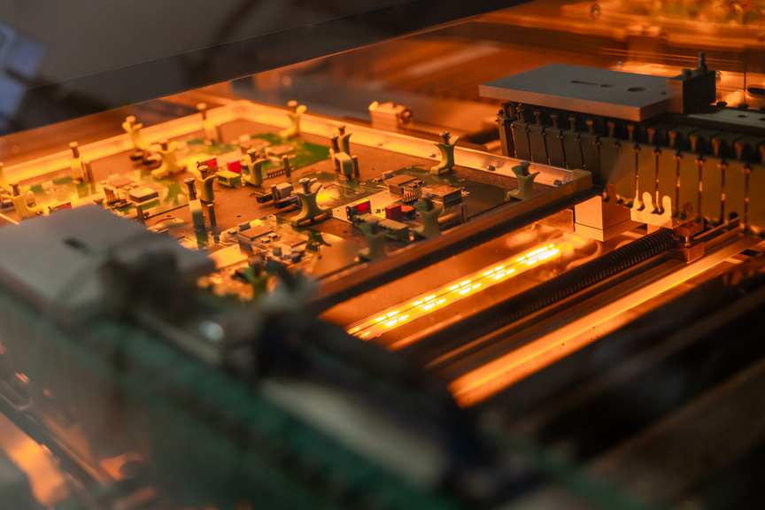
Through-Hole Assembly (also known as Through-Hole Technology or THT) is a type of electronic assembly process in which components with leads (or pins) are inserted into holes drilled through a printed circuit board (PCB) and soldered on the opposite side. This is one of the traditional methods of mounting electronic components and is particularly well-suited for components that require a more robust mechanical connection, or for applications that involve heavy-duty components, power devices, or high-stress environments.
While Surface-Mount Technology (SMT) has largely replaced through-hole in modern electronics, through-hole assembly is still essential in many industries where component reliability, thermal performance, or the need for higher mechanical strength is critical.
Key Stages of Through-Hole Assembly
Through-hole assembly is a multi-step process that includes component insertion, soldering, inspection, and testing. Here’s an overview of each step in the process:
Before the components can be inserted into the PCB, the PCB itself must be prepared.
PCB Fabrication
- A PCB designed for through-hole components will have drilled holes in specific locations based on the component’s lead placement. These holes are created during the PCB fabrication process.
- The vias (through-holes that connect layers of a multi-layer PCB) or plated through-holes (PTH) are created by drilling holes and then plating them with copper to allow electrical connections.
Solder Mask and Surface Treatment
- After the PCB is drilled, a solder mask is applied to protect the copper traces and pads from unwanted solder during the assembly process. The areas where components will be inserted remain exposed.
- Surface finishes like HASL (Hot Air Solder Leveling), ENIG (Electroless Nickel Immersion Gold), or OSP (Organic Solderability Preservative) are applied to the PCB pads to ensure good solderability and protection of the copper.
Component Insertion
Once the PCB is prepared, the next step is inserting the components. Through-hole components have leads that go through the holes in the PCB.
Manual Insertion
In small-scale or low-volume production, manual insertion may be used. Workers manually insert each component through the correct hole in the PCB, bending the leads on the opposite side to hold the components in place.
Automated Insertion (Wave Soldering)
- For high-volume manufacturing, automated insertion machines are often used to speed up the process. These machines can insert components into the board, and some can also automatically bend the leads after insertion to secure the components.
- Component feeders supply components from reels or trays to the insertion machine, where they are placed into the PCB holes with precise accuracy.
Lead Bending
After insertion, the component leads may need to be bent or trimmed. Lead bending machines are used for this step, particularly in automated environments, to ensure the leads are in the right position for soldering.
Soldering
Once the components are inserted and the leads are secured, the next step is soldering. There are two main methods for soldering through-hole components: wave soldering and hand soldering.
Wave Soldering
- Wave soldering is the most common method for high-volume through-hole assembly. In this process, the PCB passes over a wave of molten solder, which touches the component leads and the PCB pads, forming solid solder joints.
- The PCB is preheated to ensure proper melting of the solder, and the wave of molten solder is controlled to provide a uniform coating on the leads and pads.
- Flux is used to clean the surfaces and reduce oxidation before the solder is applied, ensuring a strong electrical connection.
Hand Soldering
- For low-volume production or for fixing defects, hand soldering may be used. A soldering iron is applied manually to the component leads and pads, and solder is fed into the joint to create a secure connection.
- This method is often used in prototyping or repairing assemblies.
Selective Soldering
For mixed-technology boards (combining both through-hole and surface-mount components), selective soldering is used. This method involves using a soldering iron or a robotic arm to selectively apply solder only to the through-hole component leads, avoiding the surface-mount areas.
Post-Soldering Process
After soldering, the PCB undergoes additional steps to ensure the assembly is clean, functional, and free from defects.
Cleaning
- After wave soldering, the PCB often has residual flux or solder dross that needs to be cleaned off. Cleaning methods may include:
- Aqueous cleaning (using water-based cleaning agents)
- Ultrasonic cleaning (to remove fine flux residues from complex areas)
- Brush cleaning (with a soft brush and solvent to remove any flux and contamination)
- This is an essential step to ensure the reliability of the solder joints and prevent corrosion.
Inspection
- Visual inspection is performed to check for issues such as:
- Cold solder joints (poor or insufficient solder)
- Solder bridges (excess solder causing short circuits between adjacent pads)
- Component misalignment (components not seated correctly)
- Automated Optical Inspection (AOI) can be used to detect common soldering issues and component placement defects.
- X-ray inspection may be used in some cases, especially when checking the solder joints under the PCB, such as in the case of hidden connections or multi-layer boards.
Final Testing
After the soldering process, thorough functional testing is performed to ensure the board operates correctly. This step includes:
Electrical Testing
- In-circuit testing (ICT) is used to check the electrical connections, verify that each component is functioning as intended, and identify any short circuits or open circuits.
- Boundary scan testing may also be used for testing ICs and ensuring all solder joints are properly connected.
Functional Testing
- The PCB is powered up, and functional tests are performed to verify that the board performs its intended tasks. This could involve checking signal integrity, communication protocols, voltage levels, and other operational parameters.
- Burn-in testing (placing the board under extended use conditions, like temperature and load) may also be used to ensure long-term reliability.
Final Inspection and Packaging
After testing, the PCB undergoes a final inspection to ensure it meets quality standards.
Visual Inspection
A final visual inspection ensures all components are properly inserted and soldered, and that there are no visible defects like misaligned components, solder bridges, or mechanical damage.
Packaging
- The final step is packaging the board for shipment or integration into a larger product. PCBs are usually packed in anti-static bags, trays, or boxes to prevent damage during transport. They may also be marked with barcodes or serial numbers for tracking and inventory management.
Advantages and Applications of Through-Hole Assembly
Advantages of Through-Hole Assembly
- Mechanical Strength: Through-hole components are more mechanically robust, making them suitable for high-stress environments or where the component leads are subject to physical stress.
- Reliability: Through-hole technology can provide more reliable electrical connections for components that need to carry high currents or have higher resistance to vibrations and shocks.
- Easier to Hand Solder: Through-hole components are generally easier to hand solder compared to small surface-mount components, making them ideal for prototyping and repair work.
- Better for Large Components: Through-hole assembly is often preferred for large components, such as connectors, capacitors, and power devices, which may not be suitable for surface-mount assembly.
Applications of Through-Hole Assembly
- Industrial Equipment: In harsh environments, such as factories or outdoor settings, through-hole components are more durable and less likely to suffer from mechanical failures.
- Automotive: Through-hole technology is often used for power circuits and control systems where reliability and durability are essential.
- Consumer Electronics: Although SMT has largely replaced THT in many consumer electronics, through-hole components are still used in power supplies, amplifiers, and some specific high-power or high-reliability applications.
- Military and Aerospace: Due to the harsh conditions in these industries, through-hole components are used for their durability, resistance to mechanical stress, and high-reliability standards.
- Medical Devices: Components that need to endure mechanical stress, temperature changes, and vibration are often through-hole mounted, especially in life-critical equipment.