

Schematic Capture Engineering: The Blueprint of Electronic Design
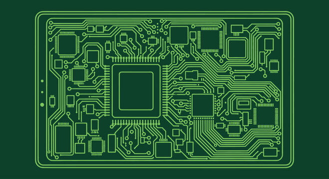
Schematic capture engineering is one of the foundational processes in the development of electronic circuits and systems. It serves as the blueprint for how electrical components are connected within a system, providing engineers with a detailed, visual representation of the design before it is physically implemented on a printed circuit board (PCB). Whether you’re designing a simple consumer gadget or a complex industrial system, schematic capture plays a critical role in ensuring the functionality, performance, and manufacturability of the final product.
In this article, we will explore the importance of schematic capture engineering, the tools and processes involved, best practices, and the role it plays in the broader context of product development.
What is Schematic Capture Engineering?
Schematic capture engineering refers to the process of creating a schematic diagram or circuit diagram that outlines the electrical connections between components in an electronic system. The schematic diagram is a visual representation of how each component interacts within a circuit, showing connections through wires or traces and defining the functional behavior of the system.
The process of schematic capture typically involves the following steps:
- Selecting Components: Choosing the right electronic components, such as resistors, capacitors, transistors, and integrated circuits (ICs), based on the design requirements.
- Component Placement: Arranging the components logically in the schematic editor, ensuring proper flow of signals and power across the system.
- Wiring Connections: Drawing the electrical connections (often represented as lines or traces) between the components to represent how they communicate and interact within the circuit.
- Simulation and Verification: Using simulation tools to verify that the design works as expected before it is turned into a physical circuit. This step ensures that there are no errors or conflicts in the schematic.
The schematic diagram produced in the capture process is then typically used as the foundation for the PCB layout, where the physical placement and routing of components take place.
The Importance of Schematic Capture Engineering
Schematic capture engineering is crucial for several reasons, making it a vital step in the electronic design process:
- Clear Communication: The schematic diagram serves as a communication tool that allows engineers, designers, and other stakeholders to understand how the circuit works. It helps ensure that everyone is on the same page, avoiding costly mistakes or misunderstandings later in the design process.
- Design Validation: By creating a schematic, engineers can check if the components are correctly connected and if the circuit meets the desired functionality. Tools for schematic capture often include built-in error-checking capabilities to ensure the design is logically sound.
- Troubleshooting: If a design fails to work correctly at any stage of development, the schematic can be used as a reference to identify issues in wiring, component selection, or connections. It becomes a blueprint for debugging and problem-solving.
- Efficiency in Development: A well-structured schematic ensures that engineers are working with an optimized and functional design, reducing the time and cost spent on redesigning faulty systems.
- Documentation and Standards Compliance: Schematic capture is part of the documentation process. Well-documented circuits help ensure compliance with industry standards and regulations. It also allows other engineers or teams to replicate or modify designs in the future.
Tools Used in Schematic Capture Engineering
Schematic capture is typically carried out using specialized Electronic Design Automation (EDA) software. These tools help automate much of the design process, ensure consistency, and improve accuracy. Some of the most widely used schematic capture tools include:
- Altium Designer: Altium is one of the most popular tools used by engineers for schematic capture and PCB layout. It offers a powerful, user-friendly interface and supports advanced features such as real-time design rule checking, integrated simulation, and easy component management.
- Eagle: Now owned by Autodesk, Eagle is another widely used EDA tool. It is favored for its ease of use, affordability, and accessibility for both professional engineers and hobbyists. Eagle is especially popular for small to medium-sized projects and prototyping.
- KiCad: KiCad is an open-source EDA tool that has grown in popularity due to its robust feature set and no-cost availability. It is a comprehensive tool for both schematic capture and PCB layout design.
- OrCAD: OrCAD is a widely used tool for schematic capture, simulation, and PCB layout in both professional and academic settings. It is known for its high-quality simulation capabilities and deep integration with other design tools.
- Cadence Allegro: Allegro is a high-end tool for professional PCB design, widely used in complex, high-performance electronic systems. It supports advanced features like signal integrity analysis, power integrity analysis, and multi-layer design capabilities.
The Process of Schematic Capture Engineering
The schematic capture process typically involves several stages, which help ensure that the design is robust and ready for the next steps in the development cycle.
- Requirements Gathering: Before beginning the schematic design, engineers must fully understand the requirements of the system. This involves understanding the functionality, performance specifications, power requirements, and environmental constraints of the final product.
- Component Selection: Once the requirements are clear, engineers begin selecting the appropriate components for the design. This includes resistors, capacitors, semiconductors, and connectors. Choosing the correct components is essential to meeting the performance and reliability goals.
- Schematic Design: With the components selected, the next step is to create the schematic diagram. This involves placing components in the schematic editor, defining their electrical connections, and ensuring that the circuit will meet the required specifications.
- Simulation and Testing: After the schematic is complete, engineers typically simulate the design to verify its functionality. This can include running basic functional simulations, such as checking signal flow or performing power analysis. Simulation helps identify issues that might not be apparent just by looking at the schematic, such as voltage spikes, power inefficiencies, or logic errors.
- Error Checking and Validation: EDA tools usually include automated error-checking features to ensure that the design is correct. These features highlight issues such as unconnected pins, incorrect component values, or potential shorts. Engineers review and correct these errors before proceeding.
- Creating the Bill of Materials (BOM): After finalizing the schematic, a Bill of Materials (BOM) is generated. The BOM is a comprehensive list of all components, their specifications, and quantities required for building the system. It is essential for procurement, assembly, and manufacturing.
Best Practices in Schematic Capture Engineering
To ensure a successful schematic capture and avoid common pitfalls, engineers follow several best practices:
- Organize Components Logically: Place components in the schematic to follow the signal flow logically. Group related components together and ensure power and ground connections are clear and well-managed.
- Use Consistent Naming Conventions: A consistent naming convention for components, nets, and signals improves clarity and ensures that the schematic is easy to understand for others, especially in collaborative projects.
- Incorporate Simulation Early: Simulation helps catch errors early in the design process. By running functional simulations, engineers can test key aspects of the circuit and make adjustments before moving on to physical implementation.
- Use Design Rule Checks: Enable automated design rule checks (DRC) in your EDA tool to catch errors like incorrect component values, floating pins, or unconnected nets that could cause issues later in the development process.
- Consider the Final PCB Layout: While creating the schematic, consider how the design will eventually be laid out on the PCB. This includes thinking about component placement, trace routing, and minimizing the length of critical signal paths.
- Documentation: Ensure the schematic is well-documented with labels, component values, and any other relevant information. Clear, comprehensive documentation makes it easier to hand off the design for PCB layout or to future engineers working on the system.