

PCB Layout Engineering: The Crucial Step in Electronics Design
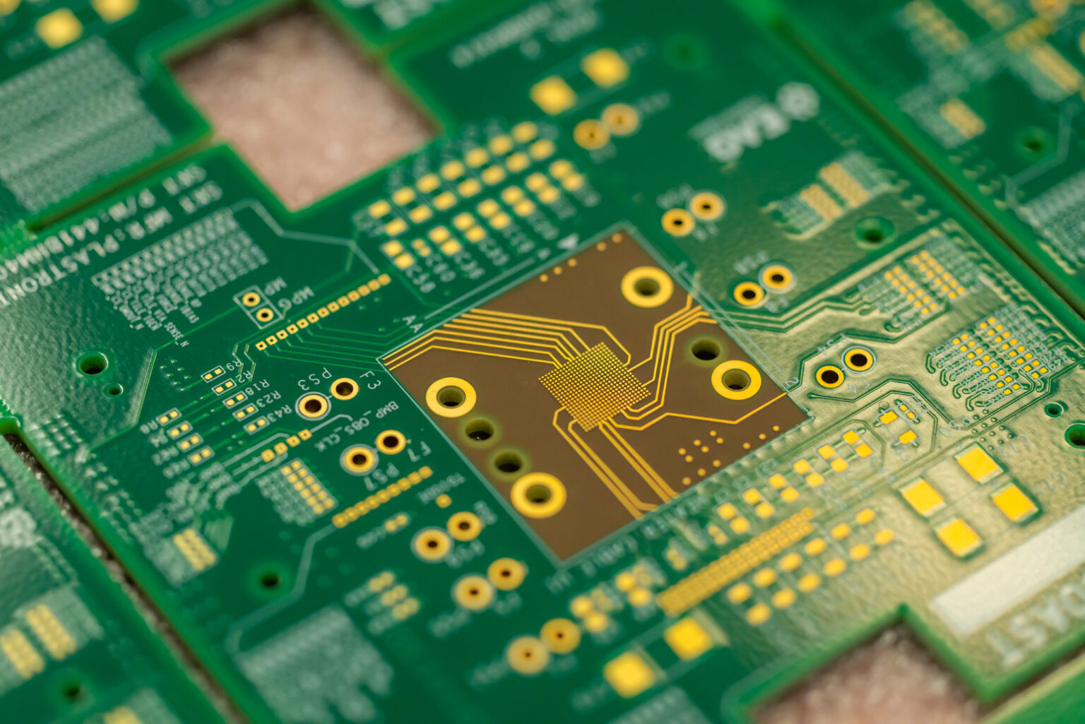
Printed Circuit Board (PCB) layout engineering is a vital aspect of electronics design, determining the physical arrangement of electrical components and their connections on a board. This step in the design process ensures that the board will function correctly, efficiently, and reliably in the final product. Whether you’re developing a consumer gadget, a medical device, or an industrial system, the quality of the PCB layout can significantly impact the performance, cost, and manufacturability of the device.
In this article, we will explore what PCB layout engineering involves, why it is crucial, the best practices involved, and how engineers can optimize designs for performance, manufacturability, and reliability.
What is PCB Layout Engineering?
PCB layout engineering refers to the process of arranging and routing the electrical components on a PCB and connecting them using conductive traces. This process is done after the schematic design, which maps out the electrical connections between components but does not address the physical placement and routing on the board.
The layout must consider a range of factors, including electrical requirements, signal integrity, thermal management, and mechanical constraints. A good PCB layout ensures that the circuit functions optimally and meets performance, reliability, and safety standards while minimizing issues like noise, heat buildup, and signal interference.
The Importance of PCB Layout Engineering
A well-executed PCB layout is crucial for the following reasons:
- Ensuring Electrical Performance: A properly designed PCB ensures that the components and signals interact with minimal interference, loss, or distortion. Poor layout can lead to issues like crosstalk, noise, and power delivery problems that affect the overall performance of the system.
- Minimizing Signal Integrity Issues: High-speed circuits are highly sensitive to signal integrity problems. PCB layout engineers use techniques such as controlled impedance routing and differential pairs to minimize issues like reflections, EMI (electromagnetic interference), and grounding problems.
- Thermal Management: Components on a PCB can generate heat during operation, and improper layout can lead to overheating, which can damage components or reduce their lifespan. A well-designed PCB layout considers thermal dissipation through component placement, heat sinks, and the use of thermal vias.
- Manufacturability and Cost Efficiency: Efficient PCB layout design ensures that the board can be produced at scale without errors or costly revisions. Optimizing component placement and minimizing the number of layers and vias helps keep manufacturing costs down.
- Compliance with Standards: Many industries have strict regulatory standards (e.g., RoHS, CE, UL) that PCBs must meet. A good layout ensures that the design complies with these standards for safety, environmental impact, and reliability.
Key Factors in PCB Layout Engineering
PCB layout engineering requires careful consideration of several factors to ensure the final board meets performance, manufacturability, and reliability standards:
- Component Placement:
- Functionality: Components should be placed in a way that aligns with the signal flow, allowing for efficient routing and minimizing the distance between related components (e.g., capacitors near power pins, components with high-frequency signals close together).
- Accessibility: Components that need regular maintenance or testing should be easy to access on the board.
- Thermal Considerations: Components that generate heat, such as power transistors or voltage regulators, should be placed in areas with sufficient space or near heat sinks to ensure proper heat dissipation.
- Routing:
- Signal Traces: Signal traces should be as short and direct as possible to minimize resistance, inductance, and capacitance, which can degrade signal quality. High-frequency signals, in particular, require careful routing to avoid interference.
- Trace Width and Spacing: Proper trace width and spacing are critical for both electrical performance and manufacturability. Trace width must be sufficient to handle the expected current without overheating, while spacing ensures that there is no short circuit between traces.
- Ground Planes: A solid ground plane reduces noise and helps with thermal management. A good PCB layout will often have dedicated ground planes that provide a low-resistance path for ground connections and minimize EMI.
- Power Distribution:
- Power Planes: Like ground planes, power planes provide a stable distribution of power across the PCB and reduce voltage drops, ensuring that power-hungry components receive the necessary current without causing instability.
- Decoupling Capacitors: Placing decoupling capacitors close to power pins of active components helps smooth out voltage fluctuations and reduce noise in the system.
- Signal Integrity:
- High-Speed Signals: For high-frequency or high-speed designs, signal integrity becomes paramount. Differential pair routing, impedance-controlled traces, and the use of via stubs should be considered to maintain signal quality.
- Minimizing Crosstalk: To reduce crosstalk between traces, high-speed signal traces should be kept apart, and proper shielding (e.g., ground planes) should be used to isolate sensitive signals.
- Thermal Management:
- Component Placement for Heat Dissipation: Components that generate significant heat should be placed away from heat-sensitive parts of the board. Thermal vias and heat sinks can be used to help spread heat across the board.
- Via Usage: Vias can be used to conduct heat away from components and redistribute it across the board, but excessive use of vias can also affect signal integrity and increase manufacturing complexity.
- Design for Manufacturability (DFM):
- Minimizing Layer Count: While complex designs may require multi-layer PCBs, a good layout will try to minimize the number of layers to reduce manufacturing complexity and cost.
- Minimizing Vias: Excessive vias can increase the complexity of manufacturing and may introduce signal integrity issues. Engineers should design PCBs that minimize the number of vias, especially blind and buried vias.
- Footprint Standards: Components should be placed in a way that adheres to standardized footprints for ease of assembly. Non-standard footprints can increase production costs and assembly errors.
Best Practices in PCB Layout Engineering
To achieve optimal PCB layouts, engineers often follow these best practices:
- Use of Design Tools: Modern PCB layout design is typically done using specialized Computer-Aided Design (CAD) tools such as Altium Designer, Eagle, KiCad, or Cadence. These tools provide powerful features for simulation, error-checking, and optimization of layouts.
- Perform Signal Integrity Analysis: For high-speed circuits, performing a signal integrity analysis during the design phase can help identify potential issues like reflections or EMI. Simulation tools can be used to verify signal behavior under different conditions.
- Follow Design Guidelines: PCB manufacturers often provide design guidelines that specify optimal trace widths, component spacing, and other factors. Following these guidelines can improve manufacturability and help prevent costly design revisions.
- Collaboration with Manufacturers: Close communication with the PCB manufacturer is key to ensuring the layout meets fabrication capabilities and is manufacturable at scale. Design-for-manufacturing (DFM) checks can help identify potential issues early in the design process.